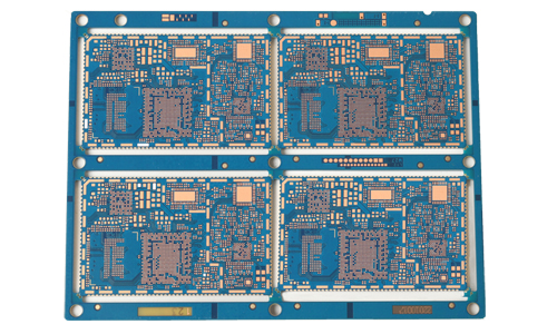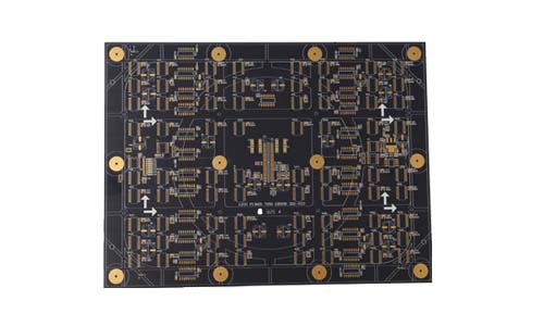
14-layer HDI (High Density Interconnect) PCB circuit board is a high-performance circuit board widely used in modern electronic devices, especially for applications with extremely high space and performance requirements, such as smartphones, tablets, medical devices and high-end computers.
HDI Arbitrary Interconnect PCB For Pico Projector Product Introduction
 |
 |
1.Product Overview
14-layer HDI (High Density Interconnect) PCB circuit board is a high-performance circuit board widely used in modern electronic devices, especially for applications with extremely high space and performance requirements, such as smartphones, tablets, medical devices and high-end computers. HDI technology can achieve higher circuit density and better electrical performance in a limited space by using designs such as micro blind vias, buried vias and fine lines.
2.Product Features
High-density design
The use of micro blind vias and buried vias greatly improves the wiring density and adapts to the needs of complex circuit design.
Allows smaller component spacing and reduces PCB size.
Superior electrical performance
Low resistance and low inductance design to ensure stability and high speed of signal transmission.
Optimized power and ground layer design to reduce electromagnetic interference (EMI) and signal crosstalk.
Multi-layer structure
14-layer design provides abundant wiring space, supports complex circuit layout and multiple function integration.
Suitable for high-frequency and high-speed signal transmission, meeting the needs of modern electronic devices.
Good heat dissipation performance
Adopt high thermal conductivity materials and reasonable hierarchical structure design to improve heat dissipation performance and ensure stable operation of equipment.
3.Technical Specifications
| Number of layers | 14 layers HDI arbitrary interconnection | Ink color | blue oil white text |
| Material | FR-4 S1000-2 | Minimum line width/line spacing | 0.075mm/0.075mm |
| Thickness | 1.6mm | Features | half-hole process |
| Copper thickness | 1oz inner layer 1OZ outer layer | Impedance control | half-hole process |
| Surface treatment | immersion gold + OSP | / | / |
4.Application Areas
Consumer electronics
Such as smart phones, tablets, game consoles, etc., to meet the needs of high performance and miniaturization.
Medical equipment
Used for high-precision medical instruments and equipment to ensure the reliability and real-time performance of data transmission.
Communication equipment
Including base stations, routers and switches, etc., supporting high-speed data transmission and stable connection.
Industrial Control
Applied to automation equipment and control systems, providing high-reliability circuit solutions.
5.Manufacturing Process
Material selection
High-frequency and high-speed materials (such as PTFE, FR-4, etc.) are used to ensure the performance and durability of the circuit board.
Printing process
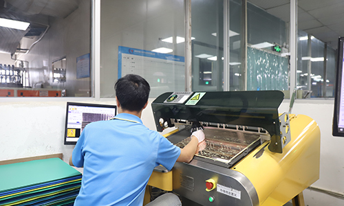
Advanced photolithography and etching technology are used to ensure the accuracy and fineness of the circuit.
Assembly process
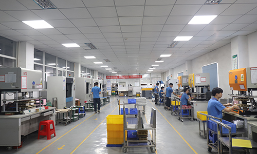
Surface mount (SMT) and through-hole mounting (THT) technology are used to ensure the firmness and reliability of components.
 |
 |
6.Quality Control
Strict testing process
Including functional testing, voltage resistance testing, thermal cycle testing, etc., to ensure the quality of each PCB.
Compliance with international standards
ISO9001, IPC-A-600 and other certifications are passed to ensure that the products meet international standards.
7.Conclusion
14-layer HDI arbitrary interconnect PCB circuit board is an indispensable core component in modern electronic devices. With its high density, high performance and superior electrical characteristics, it provides strong support for various high-end applications. Choosing the right manufacturer and material can ensure the stability and reliability of the PCB to meet the evolving market needs.
FAQ
Q: How far is your factory from the airport?
A: 30 km.
Q: What is your MOQ?
A:1 PCS.
Q: After providing Gerber, product process requirements, when can I get a quote?
A:PCB quote within 1 hour.
Q: Common problems with HDI arbitrary interconnect PCB circuit boards are as follows:
A:1 Soldering defects: Soldering defects are one of the most common problems in HDI circuit board manufacturing, which may include cold welding, solder bridging, solder cracks, etc. Solutions to these problems include optimizing soldering parameters, using high-quality solder and flux, and regularly maintaining soldering equipment.
2 Rework problems: Rework is an inevitable process in HDI circuit board manufacturing, especially when defects are found. Correct rework technology can ensure the functionality and reliability of the circuit board. Solutions to rework problems include using appropriate rework equipment, precise defect positioning, and controlling rework temperature and time1.
3 Rough hole wall: During the manufacturing process of HDI boards, improper drilling can lead to rough hole walls, affecting the performance of the circuit board. Solutions include using the right drill bit, ensuring the drilling speed is moderate, and optimizing drilling parameters to improve the hole wall quality.
4 Plating quality issues: Plating is a key link in the manufacturing process of HDI boards. Improper plating can lead to uneven conductor thickness, affecting the performance of the circuit board. Solutions include surface treatment of the substrate to remove oxides and impurities, and optimizing plating parameters to improve plating quality2.
5 Warping issues: Due to the large number of layers of HDI boards, warping problems are prone to occur during the manufacturing process. Solutions include controlling temperature and humidity, and optimizing the design to reduce the risk of warping.
6 Short circuit and open circuit: This is one of the most common types of faults. A short circuit refers to an accidental connection between two or more conductors in a circuit that should not be connected; an open circuit refers to a part of the circuit being cut off, resulting in the inability of current to flow.
7 Component damage: Component damage is also a common type of failure, which may be caused by overload, overheating, unstable voltage, etc.
8 PCB layer peeling: PCB layer peeling refers to the separation between the layers inside the circuit board. This failure is usually caused by improper welding or excessive temperature.
 The 8-Layer 2-Stage HDI Audio Server Transmission Dedicated PCB
 10-Layer 4 Stage HDI Digital Transfer PCB (3 Pcs)
 6-Layer 1-Stage HDI PCB with Immersion Gold
 14-Layer Black Solder Mask HDI PCB For High-Level Server
 12-Layer HDI Electronic PCB with For Server
 10-Layer 4 stage HDI Digital Transfer PCB