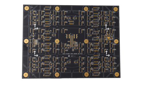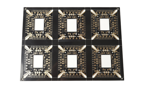
6-layer second-order PCB (printed circuit board) is a medium-complexity circuit board widely used in various electronic devices, such as consumer electronics, communication equipment, industrial control and medical equipment.
6L/8L/10L/12L Layer Second Order PCB Circuit Board Product Introduction
 |
 |
1.Product Overview
6-layer second-order PCB (printed circuit board) is a medium-complexity circuit board widely used in various electronic devices, such as consumer electronics, communication equipment, industrial control and medical equipment. Second-order PCB design usually involves multiple functional integration, which can effectively meet the needs of high performance and high density.
2.Product Features
Multi-layer structure
6-layer design provides good wiring space, suitable for the layout of complex circuits.
Optimize signal transmission and power management through reasonable layer division.
High-density wiring
Adopt fine line and micro-hole technology to achieve high-density wiring in a limited space.
Provide smaller component spacing to meet the needs of modern miniaturized equipment.
Superior electrical performance
Low resistance and low inductance design to ensure the stability and high speed of signal transmission.
Adopt multi-layer grounding and power layer design to reduce electromagnetic interference (EMI) and signal crosstalk.
Good heat dissipation performance
The design takes heat dissipation requirements into consideration, and adopts thermal conductive materials and reasonable layout to ensure stable operation of the equipment under high load.
3.Technical Specifications
| Number of layers | 6 layers HDI second order | Ink color | black oil white text |
| Material | FR-4 S1000-2 | Minimum line width/line spacing | 0.075mm/0.075mm |
| Thickness | 1.6mm | Minimum hole | 0.01 |
| Copper thickness | 1oz inner layer 1OZ outer layer | Features | hole density and line density |
| / | / | Surface treatment | immersion gold |
4.Application Areas
Consumer electronics
Such as smart phones, tablets, laptops, etc., meet the needs of high performance and miniaturization.
Communication equipment
Including routers, switches and base stations, etc., support high-speed data transmission and stable connection.
Industrial control
Used in automation equipment and control systems, providing high-reliability circuit solutions.
Medical equipment
Applied to medical instruments and equipment to ensure the reliability and real-time nature of data transmission.
5.Manufacturing Process
Material selection
Common materials include FR-4 and high-frequency materials to ensure the performance and durability of circuit boards.
Printing process
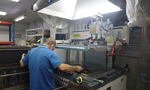
Adopt advanced screen printing and photolithography technology to ensure the accuracy and fineness of the circuit.
Assembly process
Use surface mount (SMT) and through-hole plug-in (THT) technology to ensure the firmness and reliability of components.
 |
 |
6.Quality Control
Strict testing process
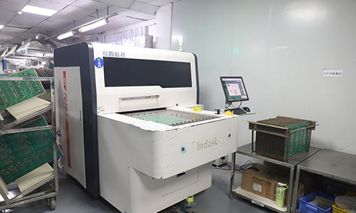
Including functional testing, voltage resistance testing, thermal cycle testing, etc. to ensure the quality of each PCB.
Compliance with international standards
Passed ISO9001, IPC-A-600 and other certifications to ensure that the products meet international standards.
7.Conclusion
The 6-layer second-order PCB circuit board is an important core component in modern electronic devices. With its high performance and multi-functional design, it provides strong support for various applications. Choosing the right manufacturer and material can ensure the stability and reliability of the PCB to meet the evolving market needs.
FAQ
Q: How far is your factory from the airport?
A: 30 km.
Q: What is your MOQ?
A: 1 PCS.
Q: Question: After providing Gerber, product process requirements, when can I get a quote?
A: PCB quote within 1 hour.
Q:Signal interference?
A: It is caused by unreasonable wiring, poor ground design or excessive power supply noise. Solutions include optimizing wiring, reasonably allocating ground and power lines, and using shielding layers or filters to reduce noise interference.
Q: Insufficient thermal design?
A:6-layer PCB generates a lot of heat when working. If the thermal design is insufficient, it may cause the circuit board to overheat and affect the normal operation of the circuit. Solutions include adding heat sinks or heat sinks, optimizing heat dissipation paths, and reasonably arranging heat dissipation components.
Q: Poor impedance matching?
A:It causes reflection and loss during signal transmission, affecting circuit performance. The solution is to use impedance calculation tools for impedance matching design, reasonably select materials and thickness, and optimize wiring.
Q: Electromagnetic compatibility issues?
A:It may cause the circuit to not work properly or even damage other equipment. The solution is to follow the EMC design specifications, lay out the ground wire and power wire reasonably, and use shielding layers and filters.
Q: Poor connector contact?
A:causes unstable signal transmission and affects circuit performance. The solution is to choose the right connector type and specification, ensure that the connector is firmly installed, and regularly check and maintain the connector.
Q: Soldering problems?
A:may cause the circuit to not work properly, or even damage the circuit board. The solution is to use high-quality solder and solder paste, ensure the correct soldering process, and regularly check and maintain the soldering quality.
Q: Poor solderability?
A:may be caused by board surface contamination, oxidation, black nickel, abnormal nickel thickness, etc. The solution includes paying attention to the process capability and quality control plan of the PCB factory, taking appropriate protective measures such as vacuum conductive bags or aluminum foil bags to prevent water vapor intrusion, and baking before use.
Q: Delamination?
A:is a common problem with PCBs, which may be caused by improper packaging or storage, material or process problems, etc. The solution includes using appropriate packaging and protective measures, and baking when necessary.
Q: Short circuit and open circuit?
A:It is a common fault type, which may be caused by improper welding or excessive temperature, resulting in PCB layer peeling. Solutions include optimizing welding process and temperature control, as well as regular inspection and maintenance.
Q: Component damage?
A:It may be caused by overload, overheating, unstable voltage, etc. Solutions include reasonable layout and use of appropriate protection measures, as well as regular inspection and maintenance of circuit boards.