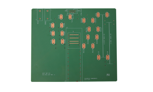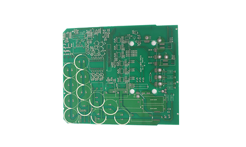
The 8-layer base station high-speed PCB circuit board is a high-performance printed circuit board designed for communication base stations and high-frequency applications.
High-rise Base Station PCB Product Introduction
The 8-layer base station high-speed PCB circuit board is a high-performance printed circuit board designed for communication base stations and high-frequency applications. The product adopts a multi-layer structure, optimizes signal transmission and power management, and is widely used in wireless communication, data transmission, and network equipment.
 |
 |
2.Main Features
8-layer design:
Adopts an 8-layer PCB structure to provide better signal integrity and power distribution.
Effectively reduces signal interference and crosstalk, and improves overall performance.
High-speed signal transmission:
The design supports high-speed signal transmission, suitable for high-frequency communication applications such as 5G and 4G.
Adopts microstrip and stripline design to optimize the signal path.
High-frequency materials:
Use high-frequency materials (such as PTFE, FR-4, etc.) to ensure stability and reliability in high-frequency environments.
Possess good dielectric properties and reduce signal attenuation.
Excellent thermal management:
The design takes thermal management into consideration to ensure effective heat dissipation in high-power applications.
Adopts thermal conductive materials to improve heat dissipation performance and extend product life.
Multiple surface treatments:
Provide multiple surface treatment options, such as ENIG, HASL, OSP, etc. to meet different customer needs.
Adapt to different welding processes and environmental requirements.
3.Technical Specifications
| Number of layers | 8 layers HDI first order | Ink color | green oil white text |
| Material | FR-4 Taiguang EM890K | Minimum line width line spacing | 0.1mm/0.1mm |
| Thickness | 1.6mm | Dielectric constant | 1oz inner layer 1OZ outer layer |
| Copper thickness | 1oz inner layer 1OZ outer layer | Surface treatment | OSP |
4.Application Areas
Base station equipment: motherboards and RF modules for wireless communication base stations.
Network equipment: suitable for high-frequency network equipment such as routers and switches.
Data transmission: various electronic devices that support high-speed data transmission.
Internet of Things: realize efficient signal processing and transmission in Internet of Things devices.
 |
 |
5.Conclusion
The 8-layer base station high-speed PCB circuit board is a high-performance and reliable product designed to meet the needs of modern communication technology. Its multi-layer structure and high-speed signal transmission capability make it an ideal choice for base stations and high-frequency applications, providing stable support for wireless communication and data transmission.
FAQ
Q: How far is your factory from the nearest airport?
A: About 30 kilometers.
Q: What is your minimum order quantity?
A: One piece is enough to place an order.
Q: How to resolve short circuits and open circuits in communication PCBs?
A: Short circuits and open circuits are usually caused by circuit aging or manufacturing defects, and need to be resolved through careful inspection and professional repair methods.
Q: Can you do nickel-palladium gold processing?
A: Yes, we can.
 10-Layer High-Frequency & High-Speed Communication PCB
 6-layer 5G Communication System AC PCB
 12-layer Second-Generation Communication Receiver System Dedicated AC PCB
 14-layer Communication Receiving AC PCB
 4-Layer PCB for Small Optical Communication Instruments
 2-Layer Communication 5G Antenna PCB