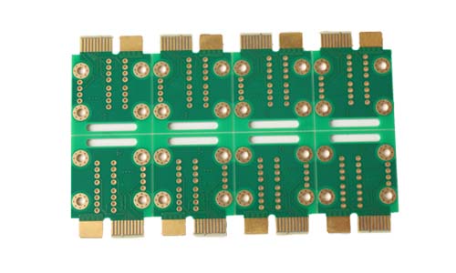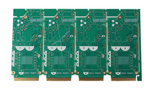
The four-layer electronic industry gold finger PCB circuit board is a high-performance printed circuit board widely used in the connection and signal transmission of electronic equipment.
Goldfinger PCB For Electronics Industry Product Introduction
 |
 |
1.Product Overview
The four-layer electronic industry gold finger PCB circuit board is a high-performance printed circuit board widely used in the connection and signal transmission of electronic equipment. The product adopts the gold finger design to ensure excellent electrical contact and durability, and is suitable for various industrial applications, including communication equipment, computer hardware and automation control systems.
2.Main Features
Four-layer structure:
Adopt four-layer PCB design to provide better signal integrity and power management.
Effectively reduce signal interference and crosstalk, and improve overall performance.
Gold finger design:
The gold finger part adopts high-quality metal materials to ensure good conductivity and wear resistance.
Provide reliable connection, suitable for application scenarios with frequent plugging and unplugging.
High temperature resistance:
Adopt high temperature resistant materials to adapt to various industrial environments and ensure long-term stable operation.
Suitable for high temperature and high humidity working conditions.
Precision manufacturing process:
Adopt advanced manufacturing process to ensure the accuracy and reliability of the line.
Have good anti-electromagnetic interference ability, suitable for high-frequency applications.
Multiple surface treatments:
Provide multiple surface treatment options, such as HASL, ENIG, OSP, etc. to meet different customer needs.
Adapt to different welding processes and environmental requirements.
3.Technical Specifications
| Number of layers | 4 layers | Ink color | green oil white text |
| Material | FR-4, S1000 | Minimum line width/line spacing | 0.1mm/0.1mm |
| Thickness | 1.6mm | Gold finger thickness | 30 wheat |
| Copper thickness | inner 0.5 outer layer 1OZ | Surface treatment | immersion gold |
4.Application Areas
Communication equipment: routers, switches, base stations, etc.
Computer hardware: motherboards, graphics cards, storage devices, etc.
Automation control: industrial controllers, sensors, actuators, etc.
Consumer electronics: smart homes, audio equipment, etc.
 |
 |
5.Conclusion
The four-layer electronic industrial gold finger PCB circuit board is a high-performance and reliable product suitable for various industrial and electronic applications. Its gold finger design and excellent electrical performance make it an ideal choice for connection and signal transmission, providing customers with a stable solution.
FAQ
Q: Do you have an office address that could be visited?
A: Our office address is Tianyue Building, Bao 'an District, Shenzhen.
Q: Will you attend the exhibition to show your products?
A: We are planning on it.
Q: Can lead residue occur after etching for gold finger PCB?
A: For thick gold fingers, lead residues can be removed. This means that if the etching process is properly operated, the problem of lead residue can be reduced or eliminated.
Q: Do you have laser drilling machines?
A: We have the most advanced laser drilling machine in the world.