6-layer 3-stage HDI PCB widely used in communications, computers, consumer electronics and other fields.
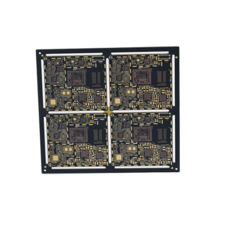
16-layer 3-level HDI PCB Product Introduction
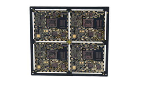
1.Product Overview
6-layer 3-stage HDI PCB widely used in communications, computers, consumer electronics and other fields. It is designed to meet the needs of modern electronic devices for high speed, high frequency and high density.
2.Product Features
1.High layer count design:
2.16-layer structure, which can support complex circuit design and multi-function integration.
3.HDI technology:
4.Adopting high-density interconnect technology, it can achieve smaller line spacing and higher line density.
Supporting micro blind hole and buried hole technology, improving the reliability of signal transmission.
5.Superior electrical performance:
6.Low resistance and low inductance characteristics, suitable for high-speed signal transmission.
Optimized stacking structure, reducing signal interference and crosstalk.
7.Good heat dissipation performance:
8.Adopting high thermal conductivity materials to ensure heat dissipation under high load operation.
9.Multiple material options:
10.Different substrates can be provided according to customer needs, such as FR-4, Rogers, etc.
3.Application Areas
Communication equipment: such as base stations, routers, switches, etc.
Consumer electronics: such as smart phones, tablets, game consoles, etc.
Industrial equipment: such as automation control systems, medical equipment, etc.
Automotive electronics: such as in-vehicle entertainment systems, navigation systems, etc.
4.Technical Parameters
| Product name | 16-layer 3-step HDI PCB | Line width and spacing | 4MIL/4MIL |
| Product use | module | Via | 0.2MM |
| Board thickness | 2.0MM | Impedance control | +/-8% |
| Color | green oil and white characters | Surface treatment process | immersion gold 2U |
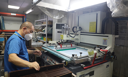
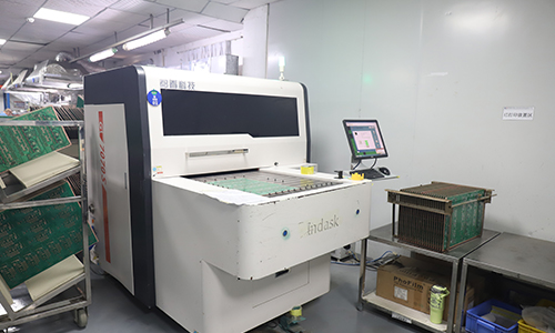
5.Production Process
Precision etching: ensure the fineness and accuracy of the line.
Multi-layer lamination: achieve the stability of multi-layer boards through high temperature and high pressure processes.
Surface treatment: provide a variety of surface treatment methods, such as HASL, ENIG, etc. to meet different needs.
 |
 |
6.Quality Control
Strict testing standards: including electrical performance testing, thermal cycle testing, mechanical strength testing, etc.
ISO certification: meet international standards to ensure product quality and reliability.
7.Summary
16-layer 3-level HDI is an indispensable core component in modern electronic products. With its high performance, high density and superior electrical characteristics, it meets the needs of various high-end applications. We are committed to providing customers with high-quality HDI PCB solutions to help customers gain an advantage in the fierce market competition.
FAQ
1.Q: How far is your factory from the nearest airport?
A: About 30 kilometers
2.Q: What is your minimum order quantity?
A: One piece is enough to place an order.
3.Q: When can I get a quotation after I provide Gerber, product process requirements?
A: Our sales staff will give you a quotation within 1 hour.
4.Q. What are the common problems for HDI arbitrary interconnect PCB circuit board?
A: There are the following questions:
1)Welding Defects: Welding defects are one of the most common problems in HDI circuit board manufacturing and may include cold welding, welding bridging, and welding cracks. Solutions to these problems include optimizing soldering parameters, using high-quality solder and flux, and regular maintenance of welding equipment.
2)Rework problems: Rework is an inevitable process in HDI circuit board manufacturing, especially when defects are found. Proper rework techniques can ensure the function and reliability of the board. Solutions to rework problems include the use of appropriate rework equipment, accurate defect location, and control of rework temperature and time.
3)Rough Hole Walls: In the HDI board manufacturing process, improper drilling of holes can lead to rough hole walls, affecting board performance. Solutions include using the right drill bit and ensuring that the drilling speed is moderate, as well as optimizing drilling parameters to improve hole wall quality.
4)Plating quality problems: plating is a key part of the HDI board manufacturing process, improper plating will lead to uneven conductor thickness, affecting the performance of the board. Solutions include surface treatment of the substrate to remove oxides and impurities, and optimization of plating parameters to improve plating quality.
5)Bow problem: Due to the high number of layers in HDI boards, warpage problems are likely to occur during the manufacturing process. Solutions include controlling temperature and humidity, and optimizing design to reduce the risk of warpage.
6)Short circuits and circuit breakers: This is one of the most common types of faults. A short circuit is an unintended connection between two or more conductors in a circuit that should not be connected; a circuit breaker is a part of the circuit that is cut off, resulting in a failure of current flow. A short circuit is an accidental connection between two or more conductors in a circuit that should be connected.
7)Component damage: component damage is also one of the common types of failure, may be due to overload, overheating, voltage instability and other reasons.
8)PCB layer peeling: PCB layer peeling refers to the circuit board within the layer and the layer between the phenomenon of separation. This kind of failure is usually caused by improper welding or high temperature.
 The 8-Layer 2-Stage HDI Audio Server Transmission Dedicated PCB
") 10-Layer 4 Stage HDI Digital Transfer PCB (3 Pcs)
10-Layer 4 Stage HDI Digital Transfer PCB (3 Pcs)
 6-Layer 1-Stage HDI PCB with Immersion Gold
 14-Layer Black Solder Mask HDI PCB For High-Level Server
 12-Layer HDI Electronic PCB with For Server
 10-Layer 4 stage HDI Digital Transfer PCB