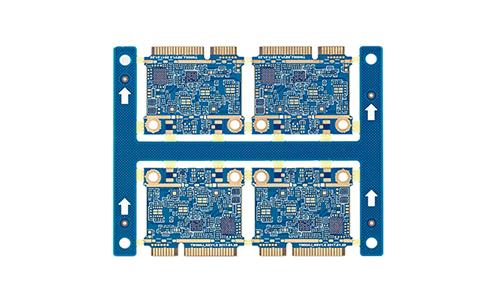
10-layer 3-level HDI gold finger PCB designed for applications that require high-density connections and excellent electrical performance.
10-Layer 3-Level HDI Gold Finger PCB Product Introduction

1.Product Overview
10-layer 3-level HDI gold finger PCB designed for applications that require high-density connections and excellent electrical performance. Gold fingers refer to the metal connection part on the edge of the PCB, which is usually used to insert connectors to ensure the reliability of electrical connections.
2.Product Features
1.High-layer design:
2.10-layer structure, which can support complex circuit design and is suitable for multi-functional integration.
3.HDI technology:
4.Adopting high-density interconnection technology, the line spacing is smaller and the line density is higher.
Supporting micro blind hole and buried hole technology to improve the reliability of signal transmission.
5.Gold finger design:
6.The gold finger part uses high conductive materials to ensure excellent electrical connection.
Surface metallization treatment enhances wear resistance and oxidation resistance.
7.Superior electrical performance:
8.Low resistance and low inductance characteristics, suitable for high-speed signal transmission.
Optimized stacking structure to reduce signal interference and crosstalk.
9.Good heat dissipation performance:
10.High thermal conductivity materials are used to ensure heat dissipation under high load.
3.Application Areas
Communication equipment: such as base stations, routers, switches, etc.
Consumer electronics: such as smart phones, tablets, game consoles, etc.
Industrial equipment: such as automatic control systems, medical equipment, etc.
Automotive electronics: such as in-vehicle entertainment systems, navigation systems, etc.
4.Technical Parameters
| Number of layers | 10L | Inner copper thickness | 35μm |
| Board thickness | 1.0mm | Outer copper thickness | 35μm |
| Minimum aperture | 0.1mm | Surface treatment | Gold+Gold finger+Bevel ENIG+OSP+Beveling of G/F |
| Minimum line width/line spacing | 0.075mm/0.075mm | Minimum distance from hole to line | 0.16mm |
5.Production Process
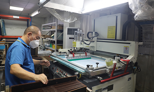
Precision etching: Ensure the fineness and accuracy of the line.
Multi-layer lamination: The stability of the multi-layer board is achieved through high temperature and high pressure process.
Surface treatment: The gold finger part can be treated with gold plating, nickel plating and other treatments to improve connection performance and durability.
 |
 |
6.Quality Control
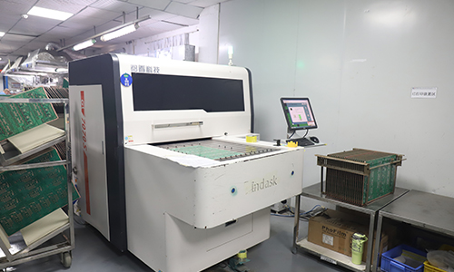
Strict testing standards: including electrical performance test, thermal cycle test, mechanical strength test, etc.
ISO certification: in line with international standards to ensure product quality and reliability.
7.Summary
The 10-layer 3-level HDI gold finger PCB is an indispensable core component in modern electronic products. With its high performance, high density and superior electrical characteristics, it meets the needs of various high-end applications. We are committed to providing customers with high-quality HDI PCB solutions to help customers gain an advantage in the fierce market competition.
FAQ
1.Q: How many employees do you have in your factory?
A: More than 500.
2.Q: Are the materials you use environmentally friendly?
A: The materials we use are in accordance with ROHS standard and IPC-4101 standard.
3.Q: Will there be lead residue after gold finger PCB etching?
A: Our thick gold finger can remove the lead residue.
4.Q: Gold finger PCB will surface staining?
A: The surface of the gold finger may be stained, which will affect its normal function and use. The solution to this problem includes cleaning with appropriate cleaning agents, such as IPA solution, anhydrous ethanol, and so on. These cleaning methods can effectively remove dirt from the surface of the gold finger and restore its normal function.
5.Q: What is the main difference between first-order and second-order HDI boards?
A: First-order HDI boards undergo one pressing, one drilling, one outer copper foil pressing and one laser drilling; while second-order HDI boards add additional pressing and laser drilling steps on top of that, undergoing two pressing, two drilling and two laser drilling processes, with more complex electrical connections and higher interlayer interconnection density.
6.Q: How to design and fabricate blind holes?
A: The design and production of blind-embedded holes is one of the key technologies for HDI boards. The non-crossing nature of the holes needs to be taken into account in the design and fabrication to ensure the feasibility of fabrication and reduce production costs.
7.Q: How to detect and repair defects in third-order HDI circuit boards?
A: In the production process of third-order HDI circuit boards, the boards need to undergo strict quality inspection to ensure that the products are qualified. Commonly used inspection methods include optical inspection, X-ray inspection and ultrasonic inspection. Through these inspection methods, defects on the circuit board, such as short circuits, open circuits, misalignments, etc., can be effectively detected.
Once the defects are found, they need to be repaired in time. Repair methods include laser repair, electrochemical repair and mechanical repair. Care needs to be taken to protect the surrounding normal circuit parts during the repair process to avoid secondary damage.
 The 8-Layer 2-Stage HDI Audio Server Transmission Dedicated PCB
 10-Layer 4 Stage HDI Digital Transfer PCB (3 Pcs)
 6-Layer 1-Stage HDI PCB with Immersion Gold
 14-Layer Black Solder Mask HDI PCB For High-Level Server
 12-Layer HDI Electronic PCB with For Server
 10-Layer 4 stage HDI Digital Transfer PCB