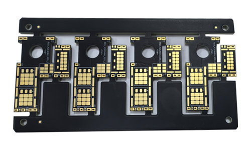
10-layer HDI (high-density interconnect) 2-order multilayer designed for applications that require high-density connections and complex circuit designs.
10-Layer 2-Order HDI Multilayer PCB Product Introduction

1.Product Overview
10-layer HDI (high-density interconnect) 2-order multilayer designed for applications that require high-density connections and complex circuit designs. This product is widely used in consumer electronics, communication equipment, industrial control and other fields, and can meet the requirements of modern electronic products for miniaturization, high performance and high reliability.
2.Product Features
1.High-layer design:
2.10-layer structure, supports complex circuit design, suitable for multi-function integration and high-density wiring.
3.HDI technology:
4.Adopting high-density interconnect technology, the line spacing is smaller, the line density is higher, and the space utilization is optimized.
Support micro blind hole and buried hole technology to improve the reliability of signal transmission.
5.2-order multilayer design:
6.The 2-order multilayer structure can effectively reduce signal transmission delay and optimize electrical performance.
Suitable for high-frequency applications, reduce signal interference and crosstalk.
7.Superior electrical performance:
8.Low resistance and low inductance characteristics, suitable for high-speed signal transmission.
Optimized stacking structure to ensure signal integrity.
9.Good heat dissipation performance:
10.Use high thermal conductivity materials to ensure heat dissipation under high load and extend product life.
3.Application Areas
Consumer electronics: such as smart phones, tablets, game consoles, etc.
Communication equipment: such as base stations, routers, switches, etc.
Industrial control: such as automation equipment, medical equipment, etc.
Automotive electronics: such as in-vehicle entertainment systems, navigation systems, etc.
4.Technical Parameters
| Material | S1000-2M | Ink color | matte black |
| Number of layers | 10 layers | Character color | white |
| Board thickness | 2.4mm-1.4mm | Surface treatment | immersion gold |
| Minimum aperture | 0.1mm | Special process | multi-layer |
5.Production Process
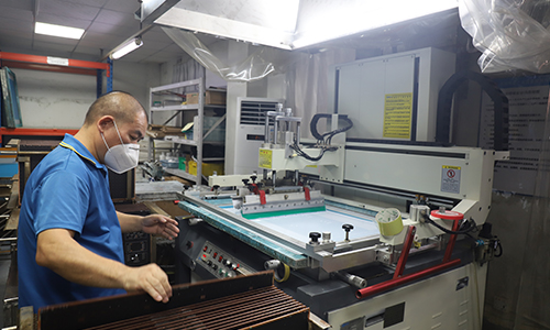
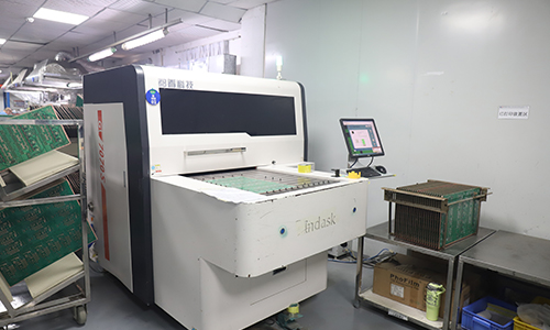
Precision etching: ensure the fineness and accuracy of the line to meet the requirements of high-density wiring.
Multi-layer lamination: achieve the stability and reliability of multi-layer boards through high temperature and high pressure processes.
Surface treatment: provide a variety of surface treatment methods, such as HASL, ENIG, etc., to meet different needs.
 |
 |
6.Quality Control
Strict testing standards: including electrical performance testing, thermal cycle testing, mechanical strength testing, etc., to ensure product reliability.
ISO certification: in line with international standards to ensure product quality and consistency.
7.Summary
10-layer HDI 2-order multilayer PCB is an indispensable core component in modern electronic products. With its high performance, high density and superior electrical characteristics, it meets the needs of various high-end applications. We are committed to providing customers with high-quality HDI PCB solutions to help customers gain an advantage in the fierce market competition.
FAQ
1.Q: How far is your factory from the nearest airport?
A: About 30 kilometers
2.Q: What is your minimum order quantity?
A: One piece is enough to place an order.
3.Q: Do you have laser drilling machines?
A: We have the most advanced laser drilling machine in the world.
4.Q: How many layers of HDI can your company produce?
A: We can produce from four layers of first order to high multi-layer arbitrary interconnect PCB circuit boards.
5.Q: What are the problems in multilayer PCB process?
A: This will involve key steps such as drilling processing, line processing. Including checking the minimum drilling hole diameter specifications, hole edge and hole edge (or slot hole) minimum spacing, hole edge and molding edge minimum distance to meet the process capability, as well as measuring the minimum line diameter, line spacing, and checking the line PAD relative to the drilling of holes with or without offset.
6.Q: What are the specific design techniques that need to be followed when stacking impedance for HDI (1st order, 2nd order, 3rd order, 4th order, any order)?
A: We need to follow the following specific design techniques: 1) We need to choose the right material. Generally, using materials with low dielectric constants can reduce the stacking impedance. In addition, we need to consider factors such as the thickness and thermal expansion coefficient of the material.
2) We need to lay out the copper foil reasonably. During the design process, we should try to avoid copper foils that are too long or too short. In addition, attention should be paid to the spacing between copper foils to ensure the stability of signal transmission.
3) We need to control the direction of the line. In the design process, we should try to avoid lines that are too zigzag or cross. In addition, attention should be paid to the distance between the lines to prevent signal interference.
7.Q: Can your company manufacture impedance boards and crimp hole PCB?
A: We can produce impedance PCBs, and the same product can be made with multiple impedance values. We can also manufacture precision holes for crimp holes.
8.Q: Can your company produce Controlled Depth PCB?
A: We can control the design of drilled holes according to the customer's drawing size requirements to ensure compliance with the customer's drawing requirements.
 The 8-Layer 2-Stage HDI Audio Server Transmission Dedicated PCB
 10-Layer 4 Stage HDI Digital Transfer PCB (3 Pcs)
 6-Layer 1-Stage HDI PCB with Immersion Gold
 14-Layer Black Solder Mask HDI PCB For High-Level Server
 12-Layer HDI Electronic PCB with For Server
 10-Layer 4 stage HDI Digital Transfer PCB