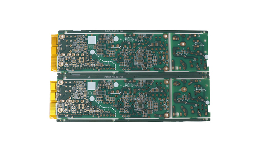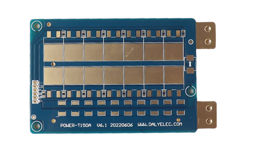
The four-layer high-power golden finger power supply PCB circuit board is a multi-layer circuit board specially designed for high-power power supplies.
4-layer High Power Goldfinger Power Supply PCB Product Introduction
The four-layer high-power golden finger power supply PCB circuit board is a multi-layer circuit board specially designed for high-power power supplies. It has high conductivity, excellent heat dissipation performance and high reliability. This PCB circuit board is widely used in servers, data centers, electric vehicle charging piles, industrial power supplies and other fields. The following is a detailed introduction to the four-layer high-power golden finger power supply PCB circuit board product.
 |
 |
1.Product Overview
The four-layer high-power golden finger power supply PCB circuit board adopts a four-layer structure design, combined with the golden finger technology, to provide efficient current transmission and excellent contact performance. The PCB circuit board can operate stably in harsh environments such as high temperature, high humidity and high vibration, ensuring the reliability and lifespan of the power system.
2. Product Features
2.1 High conductivity
Using high-quality copper foil and gold finger technology, it provides excellent conductive properties and ensures efficient transmission of high-power current.
2.2 Excellent heat dissipation performance
Through multi-layer design and reasonable heat dissipation paths, the heat dissipation capacity of PCB is significantly improved to meet the needs of high-power power supplies.
2.3 High reliability
High-quality substrates and advanced manufacturing processes are used to ensure the reliability of PCBs in harsh environments such as high temperature, high humidity, and high vibration.
2.4 High anti-interference ability
Through reasonable circuit design and shielding technology, the PCB's anti-electromagnetic interference ability is improved to ensure the stability and safety of the power system.
2.5 High integration
The four-layer design can achieve higher circuit integration, reduce the complexity and volume of the system, and improve the overall performance and reliability of the system.
3. Technical Parameters
| Number of layers | 4 | Minimum line width and line spacing | 0.3/0.3MM |
| Board thickness | 1.6mm | Minimum aperture | 0.3 |
| Board material | KB-6160 | Surface treatment | immersion gold + gold finger 30U |
| Copper thickness | inner and outer layers 2OZ | Process points | No lead residue +apply high temperature glue |
4. Application Areas
4.1 Server
Used for circuit control and power transmission of server power systems, providing high reliability and high performance power solutions.
4.2 Data center
Used for circuit control and power transmission of data center power systems to ensure efficient power conversion and stable output.
4.3 Electric vehicle charging piles
Used for circuit control and power transmission of electric vehicle charging piles, providing high reliability and long life power supply solutions.
4.4 Industrial power supply
Used for circuit control and power transmission of industrial power systems to ensure system stability and reliability.
4.5 Other high-power power supplies
Used for circuit control and power transmission of other high-power power supplies, such as UPS power supplies, inverters, etc.
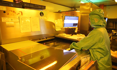
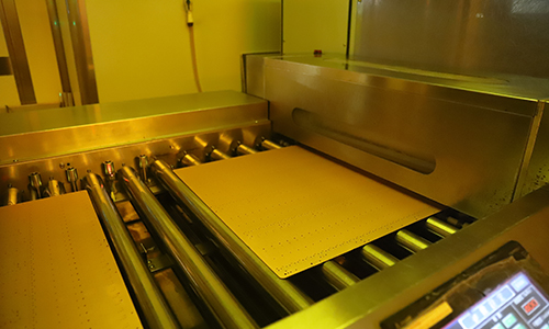
5. Manufacturing Process
5.1 Circuit design
Use EDA tools for circuit design and wiring to ensure the rationality and reliability of the circuit.
5.2 Material selection
Choose high-quality substrates and copper foil to ensure PCB performance and reliability.
5.3 Etching
Etching is performed to form a circuit pattern.
5.4 Vias
Drill holes and plate them to form vias.
5.5 Lamination
Four layers of copper foil are laminated together with the base material to form a four-layer PCB.
5.6 Surface treatment
Carry out surface treatment, such as HASL, ENIG, etc., to improve the welding performance and corrosion resistance of PCB.
5.7 Goldfinger
Gold finger processing is performed to ensure excellent contact performance and wear resistance.
5.8 Welding
Solder the components and complete the assembly.
5.9 Testing
Conduct electrical and functional tests to ensure product quality.
6. Quality Control
6.1 Raw material inspection
Ensure the quality of substrate and copper foil meets standards.
6.2 Manufacturing process control
Strictly control every process to ensure product consistency and reliability.
6.3 Finished product testing
Conduct electrical performance testing, functional testing and environmental testing to ensure that products meet design requirements.
 |
 |
7. Conclusion
The four-layer high-power golden finger power supply PCB circuit board is widely used in various high-power power supply systems due to its high conductivity, excellent heat dissipation performance and high reliability. Through reasonable design and strict manufacturing processes, efficient and reliable power solutions can be realized to meet the needs of diverse power systems.
Hope this product introduction is helpful to you!
FAQ
Q: How far is your factory from the nearest airport?
A: About 30 kilometers
Q: What is your minimum order quantity?
A: One piece is enough to place an order.
Q: How to resolve short circuits and open circuits in power PCB?
A: Short circuits and open circuits are usually caused by circuit aging or manufacturing defects, and need to be resolved through careful inspection and professional repair methods.
Q: Do you have laser drilling machines?
A: We have the most advanced laser drilling machine in the world.