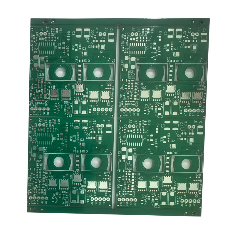
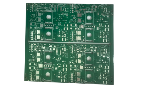
8-layer thick copper power PCB is designed for high-power and high-frequency applications, with excellent electrical performance and heat dissipation capabilities.
8-Layer Thick Copper Power PCB Product Introduction
1.Product Overview
8-layer thick copper power PCB is designed for high-power and high-frequency applications, with excellent electrical performance and heat dissipation capabilities. Its multi-layer structure and thick copper layer make it an ideal choice for fields such as power management, industrial equipment, and communication systems.
2.Product Features
1.Multi-layer structure
2.The 8-layer design enables complex circuit layouts and provides higher signal integrity and electrical performance.
3.Thick copper layer
4.The copper thickness is usually 2 oz (about 70 μm) or higher, which can carry large currents and is suitable for high-power applications.
5.Superior heat dissipation performance
6.The thick copper layer design helps to dissipate heat quickly, reduce the temperature of the circuit board, and improve the stability and reliability of the system.
7.High-frequency performance
8.Suitable for high-frequency signal transmission, reduce signal attenuation and crosstalk, and ensure signal stability.
9.Durability
10.Adopt high-quality materials with good corrosion resistance and oxidation resistance, suitable for various environmental conditions.
3.Application Fields
Power Management
Suitable for power management systems such as switching power supplies and DC-DC converters.
Industrial equipment
Widely used in industrial control, automation equipment and other fields.
Communication equipment
Suitable for high-frequency communication equipment such as base stations and communication modules.
Consumer electronics
Provide stable power support in high-performance consumer electronics products.
4.Technical Specifications
| Number of layers | 8 layers | Solder mask color | green oil and white text |
| Copper thickness | 3oz inside and outside | Minimum aperture | 0.3 mm |
| Board thickness | 3.0MM | Minimum line width | 0.2mm |
| Board material | FR-4 SY1000-2 | Surface treatment | lead-free tin spraying |
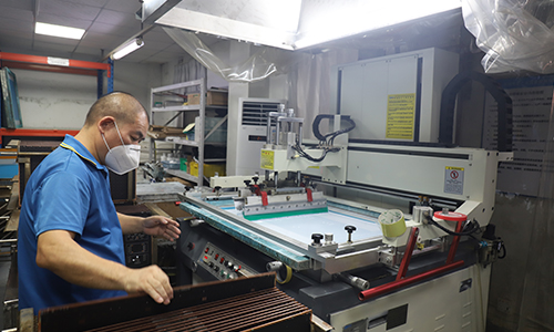
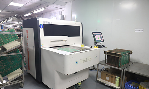
5.Production Process
1.Design phase
2.Use professional PCB design software for circuit design and layout.
3.Material selection
4.Select the appropriate substrate and copper thickness according to customer needs.
5.Manufacturing phase
6.Perform processes such as photolithography, etching, drilling, and lamination.
7.Testing phase
8.Perform electrical testing and reliability testing to ensure product quality.
9.Delivery phase
10.After completion, packaging and shipment are carried out to ensure that the product reaches the customer safely.
 |
 |
6.Conclusion
8-layer thick copper power PCB is an ideal choice for high-performance power solutions and is suitable for various high-power and high-frequency applications. With its superior electrical performance and heat dissipation capabilities, it can meet the stringent requirements of modern electronic devices for power supply.
FAQ
1.Q: What files are used in PCB production?
A: PCB production requires Gerber files and PCB manufacturing specifications, such as the required substrate material, finished thickness, copper layer thickness, solder mask color, and design layout requirements.
2.Q: When can I get a quotation after I provide Gerber, product process requirements?
A: Our sales staff will give you a quotation within 1 hour.
3.Q: How to avoid common signal interference of power PCB?
A: The need to optimize the PCB layout and reasonable planning of the ground to reduce the impact of interference.
4.Q: Can you provide samples?
A: We have the ability to quickly proof-sample PCB and provide comprehensive technical support.