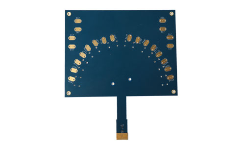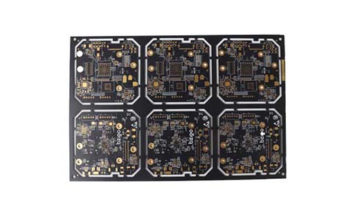
8-layer HDI (High-Density Interconnector) first-order high-speed PCB circuit board is a high-performance printed circuit board designed for high-speed signal transmission and high-density wiring.
Arduino High Speed PCB Arduino Product Introduction
 |
 |
1.Product Overview
8-layer HDI (High-Density Interconnector) first-order high-speed PCB circuit board is a high-performance printed circuit board designed for high-speed signal transmission and high-density wiring. This product adopts advanced HDI technology, with smaller aperture and higher wiring density, suitable for demanding electronic devices such as communication base stations, network equipment and high-performance computers.
2.Main Features
8-layer HDI design:
Adopt 8-layer HDI structure to provide higher wiring density and smaller signal path.
Through micro-via and blind hole technology, the space utilization of the circuit board is optimized.
High-speed signal transmission:
The design supports high-speed signal transmission and is suitable for 5G, 4G and other high-frequency applications.
Differential signal transmission and proper impedance control are used to ensure signal integrity.
High-frequency materials:
Use high-frequency materials (such as FR-4, PTFE, etc.) to ensure stability and reliability in high-frequency environments.
Possess good dielectric properties to reduce signal attenuation and delay.
Excellent thermal management:
The design takes thermal management into consideration to ensure effective heat dissipation in high-power applications.
Use thermal conductive materials and reasonable stacking structure to improve heat dissipation performance.
Multiple surface treatments:
Provide multiple surface treatment options, such as ENIG, HASL, OSP, etc., to meet different customer needs.
Adapt to different welding processes and environmental requirements.
3.Technical Specifications
| Number of layers | 8 layers | Ink color | blue oil white text |
| HDI grade | first-order HDI | Minimum line width/line spacing | 0.075mm/0.075mm |
| Material | FR-4, Taiguang EM890K | Aperture | minimum aperture 0.1mm |
| Thickness | 1.6mm | Dielectric constant | between 2.2 and 4.5 |
| Copper thickness |
inner 0.5 outer layer 1OZ |
Surface treatment | ENIG |
4.Application Areas
Communication equipment: used for wireless communication base stations, RF modules and antennas, etc.
Network equipment: suitable for routers, switches and other high-frequency network equipment.
Consumer electronics: used in high-end consumer electronics such as smartphones and tablets.
Industrial equipment: used for high-performance industrial control and automation equipment.
 |
 |
5.Conclusion
The 8-layer HDI first-order high-speed PCB circuit board is a high-performance and reliable product designed to meet the needs of modern electronic equipment for high-speed signal transmission and high-density wiring. Its advanced HDI technology and excellent electrical performance make it an ideal choice for high-frequency applications, providing stable support for various communication and network equipment.
FAQ
1.Q: What files are used in PCB production?
A: PCB production requires Gerber files and PCB manufacturing specifications, such as the required substrate material, finished thickness, copper layer thickness, solder mask color, and design layout requirements.
2.Q: When can I get a quotation after I provide Gerber, product process requirements?
A: Our sales staff will give you a quotation within 1 hour.
3.Q: How to solve the electromagnetic interference issue in industrial PCBs?
A: Use shielding and proper wiring to improve anti-interference capabilities.
4.Q: Can you manufacture HDI printed circuit board substrates?
A: We can manufacture any interconnect PCB from four-layer, one-layer to 18-layer HDI.