
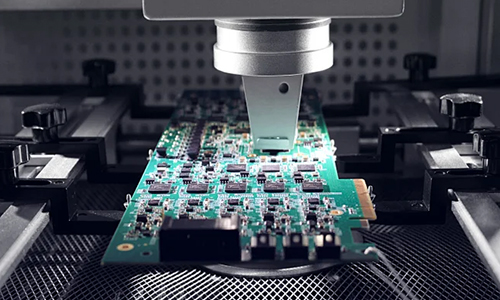
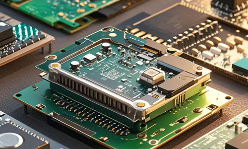
The 16-layer HDI PCB is an indispensable testing PCB for core component and equipment in the industrial control system.
Technical Specifications
| Number of layer | 16 | Minimum line width and line spacing | 0.1/0.1mm |
| Thickness of plating | 2.0mm | Minimum aperture | 0.2 |
| Board material | S1000-2M | Surface treatment | Heavy gold 3U |
| Copper thickness | Inner 1OZ Outer 1.5OZ | Process points | Impedance control + countersunk hole + resin jack |
| WHY US |
||||
 |
 |
 |
||
| Fast Delivery | High Quality | Diversified Customization | ||
| Factory | ||||
 |
 |
 |
||
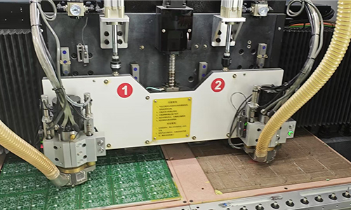
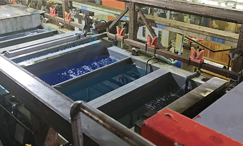
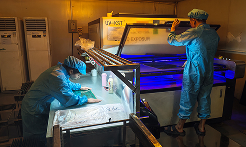
| Photoengraving Workshop | Drilling Machine | Electroplating Production Line | ||
| More Information | ||
| Strategic Partners | Application | Certificate |
FAQ
1.Q: When can I get a quotation after I provide Gerber, product process requirements?
A: Our sales staff will give you a quotation within 1 hour.
2.Q: How many employees do you have in your factory?
A: More than 500.
3.Q: How to solve the interlayer alignment error issue in automotive PCB production?
A: Interlayer misalignment errors are usually caused by inaccurate positioning systems and can be resolved by improving positioning accuracy.
4.Q: Can you provide samples?
A: We have the capability to quickly prototype PCBs and offer comprehensive technical support.