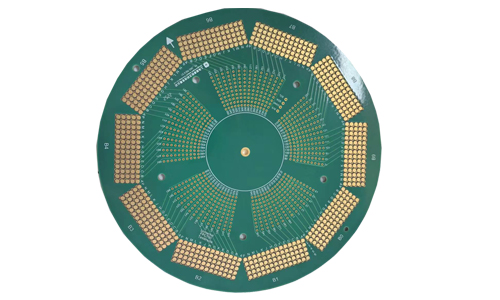
The 20-layer IC industrial control test substrate is a high-performance PCB designed for integrated circuit (IC) testing and industrial control applications.
20-Layer IC Industrial Control Test Substrate Product Introduction

1.Product Overview
The 20-layer IC industrial control test substrate is a high-performance PCB designed for integrated circuit (IC) testing and industrial control applications. The substrate adopts a multi-layer structure and advanced materials to provide excellent signal integrity, thermal management and reliability. It is widely used in automation equipment, industrial control systems, embedded systems and test equipment.
2.Product Features
1.High-density interconnection design:
2.20-layer structure supports high-density wiring, adapts to the needs of complex circuit design, and ensures the efficiency and stability of signal transmission.
3.Excellent electrical performance:
4.Use low dielectric constant (Dk) and low dielectric loss (Df) materials to optimize signal transmission, reduce signal delay and reflection, and improve overall performance.
5.Excellent heat dissipation management:
6.The heat dissipation solution is taken into consideration in the design. Through effective thermal management technology, thermal stability under high-load working conditions is ensured to extend the service life of the substrate.
7.High reliability:
8.After strict quality control and environmental testing, the reliability of the product under various harsh environmental conditions is ensured, which is suitable for industrial applications with long-term operation.
9.Powerful test function:
10.Multiple test interfaces and functional modules are integrated in the substrate design to support fast and accurate IC testing to meet the needs of different applications.
11.Flexible scalability:
12.Provide multiple interfaces and connection options, such as USB, UART, SPI, I2C, etc., to facilitate integration with other devices and modules.
3.Technical Specifications
| Number of layers | 20 layers | Ink color | green oil white text |
| Material | FR-4, SY1000-2 | Minimum line width/line spacing | 0.1mm/0.1mm |
| Thickness | 5.0mm | Is there solder mask | no |
| Copper thickness | inner 0.1 outer layer 1OZ | Surface treatment | immersion gold |
4.Application Areas
Industrial automation: used for testing and verification of control systems and automation equipment.
Embedded systems: support the development and testing of various embedded applications.
Electronic test equipment: as a test platform, used for performance evaluation and troubleshooting of integrated circuits.
IoT devices: support the development and testing of IoT related products.
5.Production Process
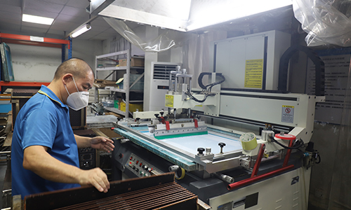
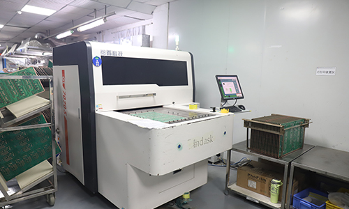
Precision etching and laser drilling: ensure the accuracy of circuit graphics to meet the design requirements of high-density interconnection (HDI).
Multi-layer lamination technology: use high temperature and high pressure process to combine different layers of materials to ensure electrical performance and mechanical strength.
Surface treatment: a variety of surface treatment methods can be selected, such as chemical gold plating (ENIG), hot air leveling (HASL), etc., to improve welding reliability and corrosion resistance.
 |
 |
6.Conclusion
The 20-layer IC industrial control test substrate has become an indispensable tool in modern industrial control and integrated circuit testing with its excellent performance, reliability and flexible application characteristics. Whether in terms of signal integrity, thermal management or test functions, the substrate has shown significant advantages, helping the development and verification of various electronic products.
FAQ
Q: What should we consider When designing this type of PCB?
A: As the following,
1. Ensure all design elements comply with IPC standards: Use automated Design Rule Check (DRC) tools to identify and correct issues.
2. Select the appropriate substrate material based on application requirements: Consider using high Tg materials to improve reliability.
3. Process capability: Communicate with the process to understand manufacturing capabilities and limitations, avoiding overly complex designs.
4. Use impedance matching techniques: Control trace width and interlayer spacing to reduce signal attenuation and reflection.
5. Design appropriate power and ground plane layouts: Use decoupling capacitors and filters to stabilize power supply.
6. Use thermal simulation tools: Predict and optimize thermal performance, select appropriate thermal management materials and designs.
7. Adhere to EMI design guidelines: Conduct EMI testing and certification.
8. Conduct reliability tests: Such as high temperature and humidity testing, thermal cycling testing, use redundant design and fault detection mechanisms.
9. Conduct thorough testing and verification during the design phase: Use automated test equipment and software to improve test efficiency and accuracy.
10. Consider cost factors in the early design stage: Optimize the design to reduce material usage and manufacturing complexity.