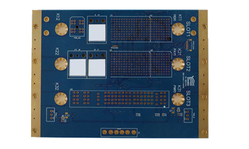
4-layer energy storage thick copper PCB is a printed circuit board designed for energy storage systems and high-power applications.
PCB For Energy Storage Product Introduction

1.Product Overview
4-layer energy storage thick copper PCB is a printed circuit board designed for energy storage systems and high-power applications. It adopts a 4-layer structure, combined with the advantages of thick copper layers, can effectively support high current and high power electrical needs, and is widely used in power management, inverters, charging piles and electric vehicles.
2.Main Features
Thick copper layer design:
Usually 1 oz to 6 oz (or higher) copper thickness is adopted, which can carry high current, reduce resistance and heat generation, and ensure the stability and safety of the circuit.
Multi-layer structure:
4-layer design provides larger wiring space, which can effectively reduce signal interference and electromagnetic interference (EMI), and improve the performance and reliability of the circuit.
Excellent heat dissipation performance:
The thick copper layer has good thermal conductivity, which can quickly conduct heat away from the heating element, reduce the operating temperature and extend the life of the component.
High-density wiring:
Suitable for high-density component layout, it can realize complex circuit design in a limited space, and meet the needs of modern energy storage equipment for miniaturization and high performance.
Good electrical performance:
Use high-quality insulating materials and reasonable stacking structure to ensure signal integrity and electrical performance, suitable for high-frequency applications.
3.Technical Parameters
| Number of layers | 4 layers | Minimum drilling | 0.2mm |
| Material | RF-4 SY1000 | Copper thickness | 3oz for inner and outer layers |
| Solder mask | blue oil white text | Board thickness | 1.6mm |
| Process | immersion gold | / | / |
4.Structure
4-layer energy storage thick copper PCB usually consists of the following parts:
Top layer (Layer 1): mainly used for signal input and output, arranging important components and connections.
Inner layer 1 (Layer 2): used for power distribution, providing stable power supply.
Inner layer 2 (Layer 3): used for signal transmission and ground wire, optimizing signal integrity and reducing interference.
Bottom layer (Layer 4): used for signal output and connection, usually with fewer components arranged.
5.Application Areas
Energy storage system: such as battery management system (BMS) and energy storage inverter.
Electric vehicles: used in battery packs and charging systems.
Power management: such as high-power power converters and drivers.
Industrial equipment: used in various high-power electronic devices and motor drives.
 |
 |
6.Conclusion
4-layer energy storage thick copper PCB has become an indispensable component in high-power energy storage devices due to its excellent heat dissipation performance, high current carrying capacity and good electrical performance. With the continuous development of energy storage technology and the increase in market demand, the application of this PCB will continue to expand, providing more efficient and reliable solutions for various industries.
FAQ
Q: What files are used in PCB production?
A: PCB production requires Gerber files and PCB manufacturing specifications, such as the required substrate material, finished thickness, copper layer thickness, solder mask color, and design layout requirements.
Q: When can I get a quotation after I provide Gerber, product process requirements?
A: Our sales staff will give you a quotation within 1 hour.
Q: How to ensure data reliability when designing a storage type PCB?
A: The key to ensuring data reliability when designing a storage type PCB lies in selecting the right storage devices and layout. High-reliability non-volatile storage devices, such as EEPROM or Flash memory, should be used, and they should be kept away from high-temperature and high-interference areas. In addition, the design should consider adequate protective measures, such as ESD protection and reverse polarity protection, as well as appropriate wiring strategies to reduce signal interference and improve data transmission stability.
Q: Do you have your own surface treatment production line?
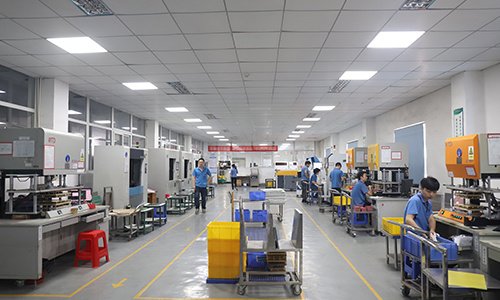
A: Sure, we have the surface treatment line.