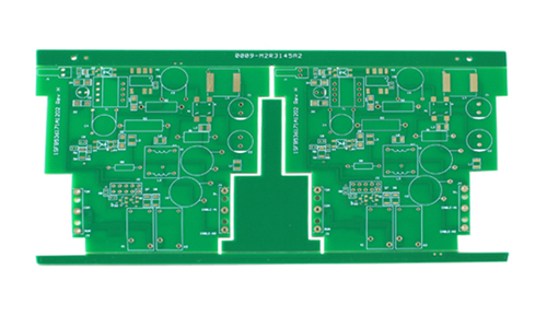
Solar inverter PCB circuit board is a printed circuit board designed for solar inverters, mainly used to convert direct current (DC) generated by solar panels into alternating current (AC) for home, industrial and commercial use.
Advanced PCB For Solar Inverter Product Introduction

1.Product Overview
Solar inverter PCB circuit board is a printed circuit board designed for solar inverters, mainly used to convert direct current (DC) generated by solar panels into alternating current (AC) for home, industrial and commercial use. The circuit board plays a vital role in solar power generation systems, ensuring efficient conversion and stable output of electrical energy.
2.Main Features
High efficiency conversion:
Design optimization for efficient DC-AC conversion, minimize energy loss and improve overall system efficiency.
High temperature and moisture resistance:
Adopt high temperature and moisture-proof materials to ensure stability and reliability under various environmental conditions, adapt to outdoor and severe weather conditions.
High current carrying capacity:
The circuit board design takes high current applications into consideration, and usually uses thick copper layers (such as 2 oz or higher) to support high power output.
Good heat dissipation performance:
Ensure temperature control of the inverter under high load conditions and extend the service life of the equipment through reasonable layout and heat dissipation design.
EMI and RFI suppression:
Shielding and filtering design is adopted to reduce electromagnetic interference (EMI) and radio frequency interference (RFI) to ensure the stability and reliability of the signal.
3.Technical Parameters
| Number of layers | 4 layers | Surface copper thickness | 35um |
| Board material | Shengyi S1000-2 | Minimum line width | 0.29mm |
| Board thickness | 1.5+/-0.1mm | Minimum line spacing | 0.21mm |
| Solder mask | green oil with white characters | Surface treatment | lead-free tin spraying |
4.Structure
Solar inverter PCB circuit board usually consists of the following parts:
Top layer (Layer 1): mainly used for input and output connections, and important components such as power switches and filters are arranged.
Inner layer 1 (Layer 2): used for power distribution and ground wire, providing stable power supply and good grounding.
Inner layer 2 (Layer 3): used for signal transmission, optimizing signal integrity and reducing interference.
Bottom layer (Layer 4): used for output connection and other auxiliary circuits, usually with fewer components arranged.
5.Application Areas
Home solar power generation system: converts solar energy into AC power that can be used by the home.
Commercial and industrial solar power systems: provide renewable energy solutions for large facilities.
Off-grid solar power systems: provide power support in places without power grids.
 |
 |
6.Conclusion
Solar inverter PCB circuit board is an indispensable component in solar power generation system. With its high efficiency conversion, high temperature resistance and moisture resistance, it ensures the effective use of solar energy. With the continuous development of renewable energy technology and the increase in market demand, the application of this PCB will continue to expand, providing more reliable solutions for global energy transformation.
FAQ
Q: How far is your factory from the nearest airport?
A: About 30 kilometers.
Q: What is your minimum order quantity?
A: One piece is enough to place an order.
Q: How to ensure data consistency during the production process of storage type PCB?
A: To ensure data consistency during the production process of storage.
Q: Can a lack of strict control during the production process lead to many problems?
A: In the production process, issues such as uneven plating thickness and inaccurate milling can negatively impact the performance of PCB. Therefore, strict control of the production process is key to ensuring quality.