
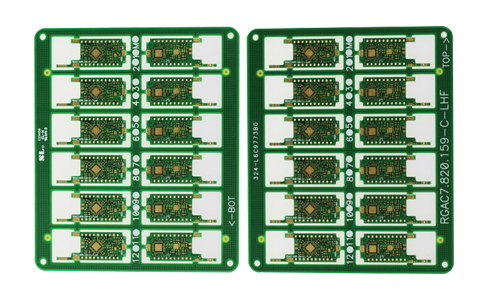
The 6-layer first-order Bluetooth PCB (printed circuit board) is designed for Bluetooth communication devices and is widely used in wireless headphones, smart homes, wearable devices and other products.
HDI PCB For Electronic Products Product Introduction
1.Product Overview
The 6-layer first-order Bluetooth PCB (printed circuit board) is designed for Bluetooth communication devices and is widely used in wireless headphones, smart homes, wearable devices and other products. This PCB ensures efficient signal transmission and stable wireless connection through multi-layer structure and fine wiring technology.
2.Product Features
1. Multi-layer design
6-layer structure: reasonable stacking design, including signal layer, ground layer and power layer, optimizes circuit layout and improves signal integrity.
Compact layout: effective use of space, suitable for miniaturized and highly integrated Bluetooth devices.
2. Superior wireless performance
Low signal loss: optimized wiring and material selection to ensure stable transmission of Bluetooth signals.
Strong anti-interference ability: through reasonable ground layer design, electromagnetic interference is reduced and communication quality is improved.
3. High thermal conductivity
Heat dissipation design: thermal conductive materials are used to ensure the stability of the device under high load and extend the service life of the product.
4. Compatibility and flexibility
Multiple Bluetooth version support: compatible with Bluetooth 5.0 and above to meet different application requirements.
Support for multiple packaging forms: Supports multiple IC packaging forms, such as QFN, BGA, etc., to flexibly respond to different design requirements.
3.Technical Parameters
| Number of layers | 6 layers | Minimum aperture | 0.1mm |
| Board thickness | 1+/-0.1mm | Surface treatment | immersion gold |
| Board material | FR-4 S1000 | Minimum hole copper | 25um |
| Solder mask | green oil with white characters | Surface copper thickness | 35um |
| / | / | Minimum line width/distance | 0.233mm/0.173mm |
4.Application Areas
Consumer electronics: wireless headphones, Bluetooth speakers, smart watches, etc.
Smart home: smart bulbs, smart sockets, home automation equipment, etc.
Medical equipment: health monitoring equipment, telemedicine equipment, etc.
Industrial applications: wireless sensors, industrial control systems, etc.
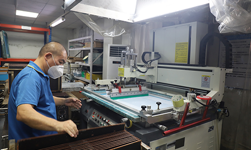
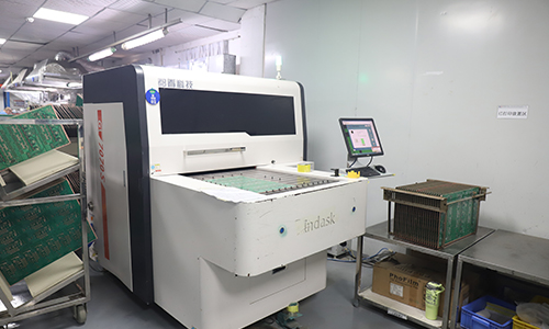
5.Production Process
High-precision manufacturing: Using advanced manufacturing equipment and processes to ensure high precision and high reliability of products.
Strict quality control: Each production link undergoes strict quality inspection to ensure that the products meet international standards.
 |
 |
6.Conclusion
6-layer first-order Bluetooth PCB is a high-performance, high-reliability circuit board solution that can meet the needs of modern wireless communication equipment for miniaturization, high performance and high integration. We are committed to providing customers with high-quality products and services to help customers succeed in the fierce market competition.
FAQ
Q: How far is your factory from the airport?
A: 30 km.
Q: What is your MOQ?
A: 1PCS.
Q: After providing Gerber, product process requirements, when can I get a quote?
A: PCB quotation within 1 hour.
4. Signal interference: It is caused by unreasonable wiring, poor ground design or excessive power supply noise.
Solutions include optimizing wiring, reasonably allocating ground and power lines, and using shielding layers or filters to reduce noise interference.
5. Inadequate thermal design: 6-layer PCB will generate a lot of heat when working. If the thermal design is insufficient, it may cause the circuit board to overheat and affect the normal operation of the circuit. Solutions include adding heat sinks or heat sinks, optimizing heat dissipation paths, and reasonably arranging heat dissipation components.
6. Poor impedance matching: It causes reflection and loss during signal transmission, affecting circuit performance. The solution is to use impedance calculation tools for impedance matching design, reasonably select materials and thickness, and optimize wiring.
7. Electromagnetic compatibility issues: It may cause the circuit to not work properly or even damage other equipment. The solution is to follow EMC design specifications, reasonably layout ground and power lines, and use shielding layers and filters.
8. Poor connector contact: It causes unstable signal transmission and affects circuit performance. The solution is to choose the right connector type and specification, ensure that the connector is firmly installed, and regularly check and maintain the connector.
9 Soldering problems: May cause the circuit to not work properly, or even damage the circuit board. The solution is to use high-quality solder and solder paste, ensure the correct soldering process, and regularly check and maintain the soldering quality.
10 Poor solderability: May be caused by board contamination, oxidation, black nickel, abnormal nickel thickness, etc. The solution includes paying attention to the process capability and quality control plan of the PCB factory, taking appropriate protective measures such as vacuum conductive bags or aluminum foil bags to prevent water vapor intrusion, and baking before use.
11 Delamination: It is a common problem of PCBs, which may be caused by improper packaging or storage, material or process problems, etc. The solution includes using appropriate packaging and protective measures, and baking when necessary.
12 Short circuit and open circuit: It is a common type of failure, which may be caused by PCB board layer peeling due to improper welding or excessive temperature. Solutions include optimizing the soldering process and temperature control, as well as regular inspection and maintenance.
13 Component damage: This may be caused by overload, overheating, unstable voltage, etc. Solutions include reasonable layout and use of appropriate protection measures, as well as regular inspection and maintenance of circuit boards


