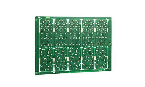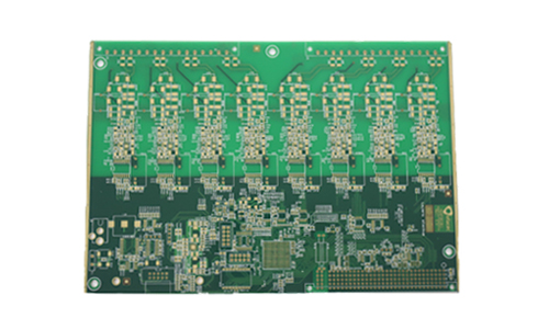
2-layer Universal Electronic Circuit Breadboard PCB is a circuit board designed for electronic prototyping and experiments. It has a double-layer structure and can provide higher connection density and more complex circuit design capabilities.
Universal Electronic PCB For Experiments Product Introduction
 |
 |
1.Product Overview
2-layer Universal Electronic Circuit Breadboard PCB is a circuit board designed for electronic prototyping and experiments. It has a double-layer structure and can provide higher connection density and more complex circuit design capabilities. Suitable for education, R&D and DIY projects, helping users to quickly build and test circuits.
2.Product Features
1. Double-layer design
High-density connection: The double-layer design allows more components and connections, suitable for the construction of complex circuits.
Better wiring capabilities: Wiring can be done between different layers, reducing interference and signal loss.
2. No-solder interface
Quick assembly: Users can easily insert and remove components without soldering, saving time.
Suitable for beginners: The no-solder design lowers the entry threshold and is suitable for electronic learning and experiments.
3. Strong compatibility
Support a variety of components: Compatible with a variety of electronic components such as resistors, capacitors, diodes, integrated circuits, etc.
Adapt to a variety of power supplies: Support a variety of voltage inputs to meet different circuit needs.
4. Durable materials
High-quality PCB materials: Made of high-quality FR-4 materials to ensure durability and stability.
Anti-oxidation treatment: Surface treatment prevents oxidation and extends service life.
3.Technical Parameters
| Number of layers | 2 | Minimum line width and line spacing | 0.4/0.4mm |
| Board thickness | 1.6mm | Minimum aperture | 0.3 |
| Board material | KB-6160 | Surface treatment | immersion gold |
| Copper thickness | 1/1oz | / | / |
4.Application Areas
Education: Used for experiments and practices in electronic courses to help students understand circuit principles.
Prototype design: Engineers can quickly verify and modify circuit designs.
DIY projects: Enthusiasts can freely combine components to create personalized circuits.
 |
 |
5.Summary
The 2-layer general electronic circuit breadboard PCB is a powerful tool suitable for a variety of electronic experiments and prototyping. Its double-layer design provides greater flexibility and connection capabilities, making it an indispensable device in education, R&D and DIY projects. Whether it is learning or development, the 2-layer breadboard can meet the needs of users.
FAQ
Q: Do You have office in shanghai or shenzhen that i can visit?
A: We are in Shenzhen.
Q: Will you attend the fair to show your products?
Answer: We're planning on it.
Q: Common problems with 3-layer general-purpose electronic circuit breadboard PCB circuit boards mainly include short circuits, open circuits, impedance mismatches, electrical noise and interference, temperature management issues, and component layout and package selection issues. How to solve these problems?
A: Short circuits and open circuits are among the most common problems with PCB circuit boards, which may be caused by incorrect wiring, soldering problems, or design errors. Short circuits can lead to incorrect signal transmission or current overload, while open circuits can cause certain circuits or components to not work properly.
Impedance mismatches may cause signal reflections, crosstalk, and signal integrity issues. This can be solved by appropriate transmission line widths, differential pairs, terminal resistors, and other measures.
Electrical noise and interference, such as cross-coupling, power supply fluctuations, ground loop problems, etc., may cause signal distortion, interference, or system instability. Methods such as shielding, filtering, and good ground plane planning should be adopted in the design to reduce electrical noise and interference.
Temperature management issues. High-power circuits or high-power devices may generate a lot of heat, and poor heat dissipation design or insufficient heat dissipation capacity may cause excessive temperature, affecting circuit performance and reliability. Proper design of heat dissipation paths, adding heat sinks or heat dissipation patches and other measures can effectively solve these problems.
Component layout and package selection. Improper component layout may cause signal interference, poor electrical isolation, and hot spot concentration. Choosing inappropriate component packages or sizes may cause welding difficulties, connection problems, or thermal management difficulties. The impact of component layout and package selection needs to be considered in PCB design.