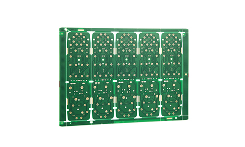
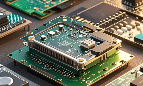
2-Layer common electronic testing PCB is a PCB designed for electronic prototyping and experiments or other electronic equipment tests. It has a double-layer structure and can provide higher connection density and more complex circuit design capabilities.
Technical Parameters
| Number of layers | 2 | Minimum line width and line spacing | 0.4/0.4mm |
| Board thickness | 1.6mm | Minimum aperture | 0.3 |
| Board material | KB-6160 | Surface treatment | immersion gold |
| Copper thickness | 1/1oz | / | / |
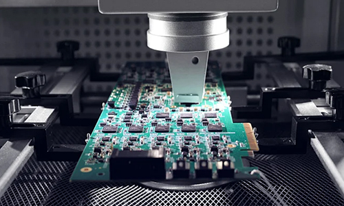
| WHY US |
||||
 |
 |
 |
||
| Fast Delivery | High Quality | Diversified Customization | ||
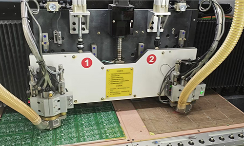
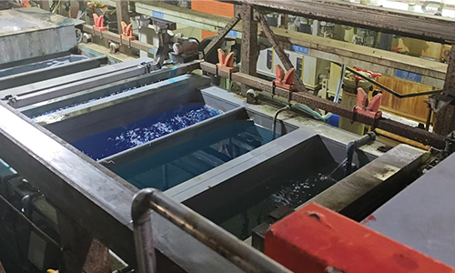
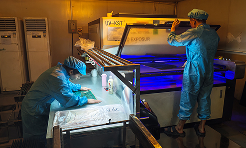
| Factory | ||||
 |
 |
 |
||
| Photoengraving Workshop | Drilling Machine | Electroplating Production Line | ||
| More Information | ||
| Strategic Partners | Application | Certificate |
FAQ:
1.Q: How far is your factory from the nearest airport?
A: About 30 kilometers
2.Q: What is your minimum order quantity?
A: One piece is enough to place an order.
3.Q: How to solve the electromagnetic interference issue in electronic PCB?
A: Use shielding and proper wiring to improve anti-interference capabilities.
4.Q: Can a lack of strict control during the production process lead to many problems?
A: In the production process, issues such as uneven plating thickness and inaccurate milling can negatively impact the performance of PCB. Therefore, strict control of the production process is key to ensuring quality.