
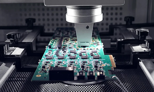
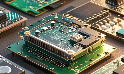
This 10-Layers HDI PCB is a base board which is widely used in electronic equipment, like computer or other electronic machine.
Technical specifications
| Number of layers | 10 layers | Ink color | black oil and white text |
| Board thickness | 1.9mm | Minimum line width / line spacing | 0.1mm / 0.1mm |
| Material | FR-4 TG170 | Impedance control | ±0.15mm |
| Copper thickness | 2oz / 1.5oz | Surface treatment | immersion gold |
| WHY US |
||||
 |
 |
 |
||
| Fast Delivery | High Quality | Diversified Customization | ||
| Factory | ||||
 |
 |
 |
||
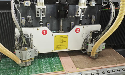
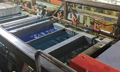
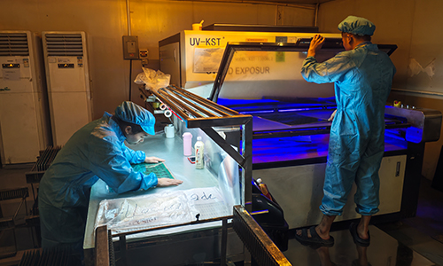
| Photoengraving Workshop | Drilling Machine | Electroplating Production Line | ||
| More Information | ||
| Strategic Partners | Application | Certificate |
FAQ
1.Q: How far is your factory from the nearest airport?
A: About 30 kilometers
2.Q: What is your minimum order quantity?
A: One piece is enough to place an order.
3.Q: What to do if solder mask overflow affects soldering quality?
A: Solder mask overflow refers to the situation where the solder mask covers the pads or vias that should be exposed, affecting the soldering quality. To address this issue, precise window settings for the solder mask should be made during the design phase and communication with the manufacturer should be confirmed to ensure their process capabilities prevent excessive overflow.
4.Q: What to do if PCB warps or deforms during manufacturing or soldering?
A: Warping and deformation of PCBs during manufacturing or soldering are due to thermal stress, which can affect assembly and functionality. Strategies to mitigate this include selecting appropriate base materials and controlling the uniformity of heating during the process. In some cases, adding stiffeners in the design can reduce the risk of warping.