
4-layer solar inverter PCB is a PCB designed for solar inverters, mainly used to convert the DC power generated by solar panels into AC power for home or industrial use.
Technical Parameters
| Number of layers | 4 layers | Surface treatment | lead-free tin spraying |
| Board material | FR4, SY1000 | Copper thickness | High-voltage DC power supply system, inner and outer layer copper thickness 2oz |
| Board thickness | 1.6mm | Hole copper thickness | 25um |
| Minimum aperture | 0.50mm | / | / |
| WHY US |
||||
 |
 |
 |
||
| Fast Delivery | High Quality | Diversified Customization | ||
| Factory | ||||
 |
 |
 |
||
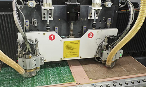
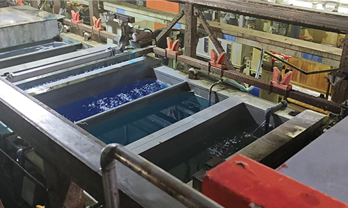
| Photoengraving Workshop | Drilling Machine | Electroplating Production Line | ||
| More Information | ||
| Strategic Partners | Application | Certificate |
FAQ
1.Q: How far is your factory from the nearest airport?
A: About 30 kilometers
2.Q: What is your minimum order quantity?
A: One piece is enough to place an order.
3.Q: How to resolve short circuits and open circuits in electronic PCB?
A: Short circuits and open circuits are usually caused by circuit aging or manufacturing defects, and need to be resolved through careful inspection and professional repair methods.
4.Q: Do you have laser drilling machines?
A: We have the most advanced laser drilling machine in the world.