
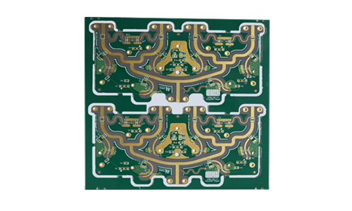
The PCB circuit board is a printed circuit board designed for high-frequency applications and is widely used in communications, radar, satellites, medical equipment and other fields.
Iron Furnace High Frequency PCB Product Introduction
1.Product Overview
The PCB circuit board is a printed circuit board designed for high-frequency applications and is widely used in communications, radar, satellites, medical equipment and other fields. The product has excellent electrical performance and thermal stability, and can meet the needs of high-frequency signal transmission.
2.Product Features
High-frequency performance
The design supports high-frequency signal transmission, with a frequency range of up to tens of GHz, suitable for high-frequency applications such as 5G and Wi-Fi 6.
High-quality substrate
The use of low dielectric constant and low-loss materials (such as PTFE, ceramic substrate, etc.) effectively reduces signal attenuation and reflection.
PCB process
The PCB welding process is used to ensure that the solder joints are firm and suitable for long-term use in high-temperature environments.
Excellent thermal stability
The design takes thermal management into consideration and can maintain stable performance under high-power working conditions.
Precision manufacturing
The use of advanced manufacturing technology ensures high line accuracy and is suitable for complex circuit design.
3.Application Areas
Wireless communication equipment
Used in base stations, routers, wireless transmission modules, etc.
Radar and satellite communications
Applied to high-frequency applications such as radar systems and satellite communications equipment.
Medical equipment
Applicable to high-frequency medical imaging equipment, monitoring instruments, etc.
Automotive electronics
Used in vehicle communication systems, autonomous driving sensors, etc.
4.Technical Parameters:
| Number of layers | 2L | Outer copper thickness | 1OZ |
| Board thickness | 0.6mm | Surface treatment | immersion gold |
| Board material | Teflon polytetrafluoroethylene | Minimum line width/line spacing | 0.12mm |
| Minimum aperture | 0.8mm | / | / |
5.Design and Manufacturing Process
Demand analysis
Communicate with customers to understand product requirements and technical specifications to ensure that the design meets high-frequency standards.
Circuit design
Use professional software for circuit design, optimize signal paths, and reduce interference.
PCB layout
Perform high-frequency layout and arrange the position of circuit components reasonably to ensure signal integrity.
Manufacturing
Use iron furnace welding process for PCB production to ensure welding quality.
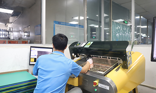
Testing and Verification
Conduct strict electrical performance tests and environmental adaptability tests on finished products to ensure that they meet design requirements.
 |
 |
Summary
The high-frequency PCB circuit board of Tiefei furnace is a key component to achieve high-frequency signal transmission. With its superior performance and broad application prospects, it has become an indispensable part of modern electronic equipment. We are committed to providing customers with high-quality products and professional technical support to meet the needs of the evolving high-frequency market.
FAQ
Q: When can I get a quotation after I provide Gerber, product process requirements?
A: Our sales staff will give you a quotation within 1 hour.
Q: How many employees do you have in your factory?
A: More than 500.
Q: How to solve the common overheating problems when using communication PCB boards?
A: The key is to introduce heat dissipation design and or choose high quality materials. For example: EMC, TUC, Rogers and other companies to provide the board.
Q: How many layers of HDI can your company produce?
A: We can produce from four layers of first order to high multi-layer arbitrary interconnect PCB circuit boards.
 10-Layer High-Frequency & High-Speed Communication PCB
 6-layer 5G Communication System AC PCB
 12-layer Second-Generation Communication Receiver System Dedicated AC PCB
 14-layer Communication Receiving AC PCB
 4-Layer PCB for Small Optical Communication Instruments
 2-Layer Communication 5G Antenna PCB


