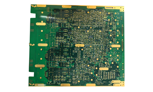
The 16-layer server motherboard is a high-performance PCB designed to meet the needs of modern servers and data centers.
Product Introduction

1.Product Overview
The 16-layer server motherboard is a high-performance PCB designed to meet the needs of modern servers and data centers. The motherboard adopts a multi-layer structure, combined with advanced materials and manufacturing processes, to provide excellent computing power, data transmission speed and system stability. It is widely used in high-performance computing (HPC), cloud computing, virtualization and big data processing.
2.Product Features
1.High-density interconnection:
2.16-layer design allows higher wiring density, supports complex circuit layout and multiple interface configurations, and meets the server's requirements for high-speed data transmission.
3.Excellent electrical performance:
4.Use low dielectric constant (Dk) and low dielectric loss (Df) materials to ensure signal stability and integrity under high-frequency conditions and optimize data transmission performance.
5.High heat dissipation efficiency:
6.The design takes heat dissipation management into consideration, and adopts a variety of heat dissipation technologies (such as heat sinks, fan interfaces, etc.) to ensure thermal stability under high-load working environments and extend the service life of the equipment.
7.Powerful scalability:
8.Provide multiple PCIe slots, SATA and M.2 interfaces, support a variety of expansion cards and storage devices, and meet the needs of different application scenarios.
9.High reliability:
10.Through strict quality control and testing, ensure the reliability of the product in various harsh environments, suitable for long-term server applications.
11.Advanced power management:
12.Integrate efficient power management solutions, support intelligent power monitoring and management, and improve the energy efficiency and stability of the system.
3.Technical Specifications
| Number of layers | 16 layers | Ink color | green oil white text |
| Material | FR-4, SY1000-2 | Minimum line width/line spacing | 0.075mm/0.075mm |
| Thickness | 2.0mm | Is there a solder mask | Yes |
| Copper thickness | inner 0.1 outer 1OZ | Surface treatment | immersion gold 2 wheat |
4.Application Areas
Data center: used to build high-performance servers, supporting large-scale data processing and storage.
Cloud computing: As the infrastructure of cloud service providers, it supports virtualization and multi-tenant environments.
High performance computing (HPC): Used for applications such as scientific computing, engineering simulation and big data analysis.
Enterprise applications: Supports databases, ERP systems and other key applications within the enterprise.
5.Production Process
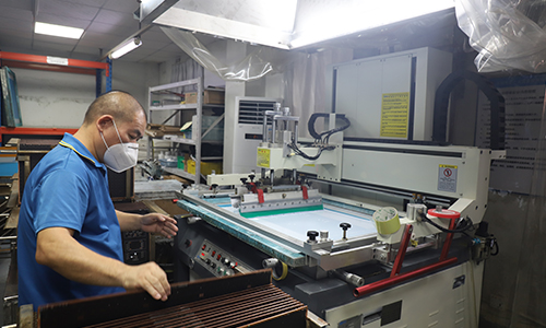
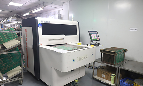
Precision etching and laser drilling: Ensure the accuracy of high-density interconnection design to meet the requirements of complex circuit layout.
Multi-layer lamination technology: Combine different layers of materials through high temperature and high pressure processes to ensure electrical performance and mechanical strength.
Surface treatment: Provide a variety of surface treatment options, such as chemical gold plating (ENIG), hot air leveling (HASL), etc., to improve welding reliability and corrosion resistance.
 |
 |
6.Conclusion
The 16-layer server motherboard has become an indispensable and important part of modern data centers and high-performance computing environments with its excellent performance, reliability and scalability. Whether in signal transmission, heat dissipation management or system stability, the motherboard has shown significant advantages, helping various high-load and high-performance applications to run smoothly.
FAQ
1.Q: What is your minimum order quantity?
A: One piece is enough to place an order.
2.Q: When can I get a quotation after I provide Gerber, product process requirements?
A: Our sales staff will give you a quotation within 1 hour.
3.Q: Why do signals sometimes become incomplete in devices equipped with communication PCBs?
A: As design complexity increases, 5G devices may utilize HDI communication PCBs with finer traces and higher-density interconnections. When transmitting high-speed signals, these finer traces may lead to incomplete signals. If such issues occur, please contact our staff to make adjustments for your product.
4.Q: What problems can be caused by inaccurate PCB design in mobile phones?
A: If the circuit design lacks a rational layout, it may lead to signal interference and unstable transmission, thereby affecting the performance of the entire phone. Therefore, we need to fully consider the position of each component and the rationality of the wiring during the PCB design phase.
5.Q: Can a lack of strict control during the production process lead to many problems?
A: In the production process, issues such as uneven plating thickness and inaccurate milling can negatively impact the performance of PCB. Therefore, strict control of the production process is key to ensuring quality.
 10-Layer High-Frequency & High-Speed Communication PCB
 6-layer 5G Communication System AC PCB
 12-layer Second-Generation Communication Receiver System Dedicated AC PCB
 14-layer Communication Receiving AC PCB
 4-Layer PCB for Small Optical Communication Instruments
 2-Layer Communication 5G Antenna PCB