
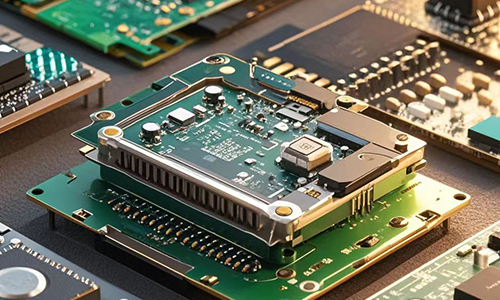
Our 8-layer communication PCB is designed for high-end communication equipment like zone integration server to meet the needs of modern network and communication systems for high-speed data transmission, stability and high-density wiring.
Technical Specifications
| Number of layers | 8 | Minimum line width and line spacing | 0.075/0.075mm |
| Board thickness | 1.6mm | Minimum aperture | 0.2 |
| Board material | S1000-2M | Surface treatment | 2” immersion gold |
| Copper thickness | 1oz inner layer 1OZ outer layer | Process points | impedance control + crimping hole |
| WHY US |
||||
 |
 |
 |
||
| Fast Delivery | High Quality | Diversified Customization | ||
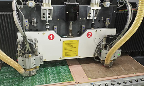
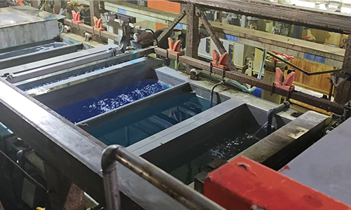
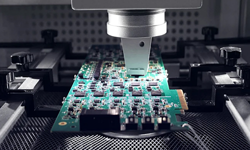
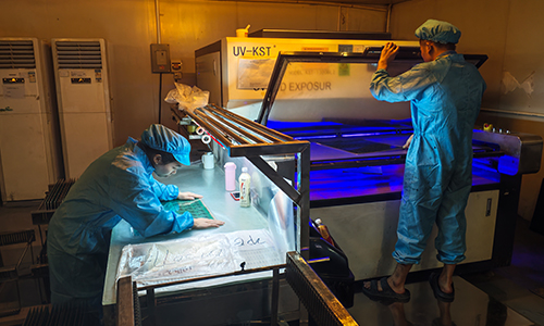
| Factory | ||||
 |
 |
 |
||
| Photoengraving Workshop | Drilling Machine | Electroplating Production Line | ||
| More Information | ||
| Strategic Partners | Application | Certificate |
FAQ
1.Q: Are the materials you use environmentally friendly?
A: The materials we use are in accordance with ROHS standard and IPC-4101 standard.
2.Q: How far is your factory from the nearest airport?
A: About 30 kilometers.
3.Q: How to avoid high-frequency and high-speed PCB circuit board common signal interference?
A: The need to optimize the PCB layout and reasonable planning of the ground to reduce the impact of interference.
4.Q: Do you have laser drilling machines?
A: We have the most advanced laser drilling machine in the world.
 10-Layer High-Frequency & High-Speed Communication PCB
 6-layer 5G Communication System AC PCB
 12-layer Second-Generation Communication Receiver System Dedicated AC PCB
 14-layer Communication Receiving AC PCB
 4-Layer PCB for Small Optical Communication Instruments
 2-Layer Communication 5G Antenna PCB


