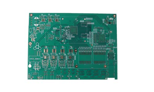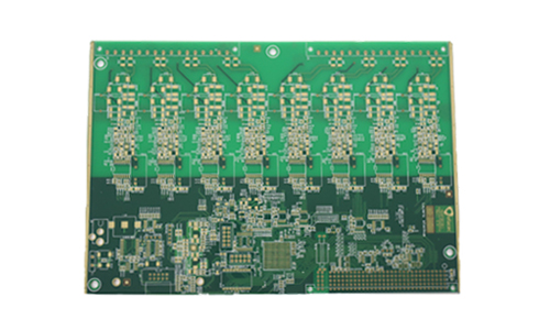
Our 8-layer communication PCB circuit board is designed for high-end communication equipment to meet the needs of modern network and communication systems for high-speed data transmission, stability and high-density wiring.
8-layer Communication PCB Circuit Board Product Introduction
 |
 |
1.Product Overview
Our 8-layer communication PCB circuit board is designed for high-end communication equipment to meet the needs of modern network and communication systems for high-speed data transmission, stability and high-density wiring. The circuit board adopts advanced manufacturing technology and high-quality materials to ensure its reliability and performance in various complex environments.
2.Main Features
8-layer structure:
Adopting 8-layer design, reasonable configuration of signal layer, power layer and ground layer, effectively reducing signal interference, improving circuit performance, suitable for communication equipment with high-density wiring.
High-frequency performance:
Adopting high-frequency FR-4 or other high-performance materials, with excellent electrical characteristics, supporting high-speed signal transmission, ensuring data stability and integrity.
Electromagnetic compatibility:
The design fully considers electromagnetic interference (EMI) and signal integrity, adopts reasonable stacking structure and shielding design to ensure stable operation in various environments.
High-quality surface treatment:
Provide a variety of surface treatment options, such as ENIG (electroplated gold), HASL (hot air leveling), etc., to ensure good welding performance and corrosion resistance to meet different application requirements.
Precision manufacturing process:
Use advanced laser drilling and high-precision lithography technology to ensure high-precision processing of tiny apertures and fine line widths, and meet the needs of high-density wiring.
Compliance with industry standards:
Products comply with industry standards such as IPC-A-600 and IPC-6012 to ensure the quality and reliability of PCBs, and are suitable for various high-end communication equipment.
3.Application Areas
Network equipment: Suitable for high-performance routers, switches and other network equipment to provide stable network connections.
Wireless communication: Widely used in wireless base stations, Wi-Fi equipment, LTE and 5G equipment, etc., supporting high-speed data transmission.
Industrial control: Used in industrial automation equipment, monitoring systems and intelligent transportation systems to ensure real-time transmission and reliability of data.
Consumer electronics: Suitable for high-tech products such as smart home devices, video surveillance, and smart speakers.
4.Technical Specifications
| Number of layers | 8 | Minimum line width and line spacing | 0.075/0.075mm |
| Board thickness | 1.6mm | Minimum aperture | 0.2 |
| Board material | S1000-2M | Surface treatment | 2” immersion gold |
| Copper thickness | 1oz inner layer 1OZ outer layer | Process points | impedance control + crimping hole |
5.Production Capacity
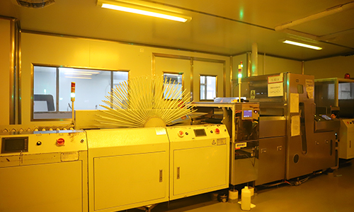
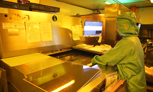
We have advanced production equipment and a professional technical team, with large-scale production capabilities to meet the diverse needs of customers. Support small-batch trial production and large-scale production, and timely delivery.
 |
 |
6.Customer Support
Provide comprehensive technical support and after-sales service to assist customers in solving various problems during the design, manufacturing and post-maintenance process to ensure the smooth progress of the project.
7.Conclusion
Our 8-layer communication PCB circuit board is an ideal choice for your high-end communication equipment development. With its high reliability, excellent electrical performance and compliance with industry standards, it helps your products stand out in the highly competitive market. For more information or to obtain a quote, please feel free to contact us.
FAQ
Q: Are the materials you use environmentally friendly?
A: The materials we use are in accordance with ROHS standard and IPC-4101 standard.
Q: How far is your factory from the nearest airport?
A: About 30 kilometers.
Q: How to avoid high-frequency and high-speed PCB circuit board common signal interference?
A: The need to optimize the PCB layout and reasonable planning of the ground to reduce the impact of interference.
Q: Do you have laser drilling machines?
A: We have the most advanced laser drilling machine in the world.
 10-Layer High-Frequency & High-Speed Communication PCB
 6-layer 5G Communication System AC PCB
 12-layer Second-Generation Communication Receiver System Dedicated AC PCB
 14-layer Communication Receiving AC PCB
 4-Layer PCB for Small Optical Communication Instruments
 2-Layer Communication 5G Antenna PCB