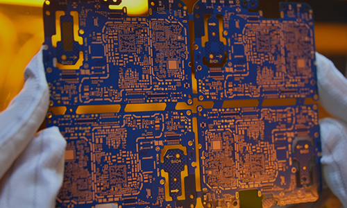
6-layer second-order HDI (high-density interconnect) PCB board is a printed circuit board designed for high-end electronic devices such as smartphones.
6 Layer HDI PCB For Mobile Phone Product Introduction

1.Product Overview
6-layer second-order HDI (high-density interconnect) PCB board is a printed circuit board designed for high-end electronic devices such as smartphones. This PCB board adopts advanced manufacturing technology, which can support complex circuit design and high-performance electronic functions, and meet the needs of modern mobile phones for miniaturization, lightweight and high performance.
2.Product Features
1. High-density interconnection
Multi-layer design: The 6-layer structure provides more wiring space, which is suitable for the design of complex circuits.
Micro-hole technology: The use of micro-hole technology (such as blind holes and buried holes) effectively improves the wiring density and reduces the PCB area.
2. Superior electrical performance
Low resistance and low inductance: Optimized circuit design and material selection ensure the high efficiency and stability of signal transmission.
High-frequency performance: Suitable for high-frequency signal transmission, meeting the needs of modern communication and data processing.
3. Light and thin design
Miniaturization: HDI technology allows PCB boards to be thinner and lighter, suitable for the design requirements of modern mobile phones.
Space saving: High-density layout reduces the footprint of PCB, leaving more space for other components.
4. Good heat dissipation performance
Heat dissipation design: Reasonable heat dissipation design ensures that the PCB can maintain a good working temperature under high load.
Thermal conductive material: Use thermal conductive material to enhance the heat dissipation effect and extend the product life.
3.Technical Parameters
| Number of layers | 6 layers | Line width/line spacing | 0.06/0.063mm |
| Product structure | 1+4+1 | Minimum laser drilling aperture | 0.1mm |
| Board thickness | 0.8±0.8mm | Surface treatment | immersion nickel gold |
| Material | EM-285 | / | / |
4.Application Areas
Smartphones: Widely used in motherboards and auxiliary circuit boards of various smartphones.
Tablets: Suitable for high-performance circuit design of tablets.
Wearable devices: Also used in smart watches and other wearable devices.
5.Production Process
1. Design: Use professional PCB design software for circuit design to ensure that the circuit is efficient and reliable.
2. Plate making: Make a photolithography plate according to the design file and perform preliminary processing of the PCB.
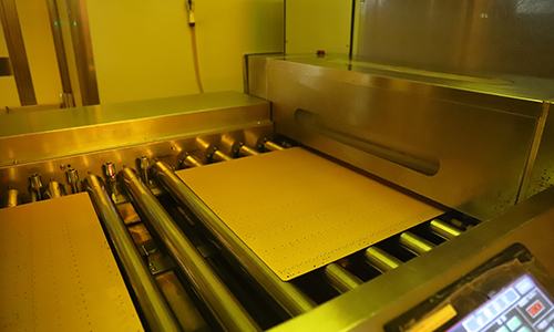
3. Etching: Remove excess copper layer to form a circuit pattern.
4. Drilling: Drill holes according to design requirements to connect circuits between different layers.
5. Surface treatment: Anti-oxidation treatment is performed to improve welding performance.
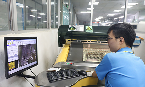
6. Testing: Electrical testing is performed to ensure product quality and performance.
 |
 |
6.Purchase Information
Suppliers: can be purchased through professional PCB manufacturers, electronic component stores or online e-commerce platforms.
Price: Depending on the size, number of layers and complexity, the price range generally ranges from a few hundred yuan to a few thousand yuan.
7.Summary
6-layer second-order HDI PCB board is an indispensable key component in modern mobile phones. With its high-density design and superior electrical performance, it is widely used in smartphones and other high-end electronic devices. It not only meets the needs of miniaturization and lightweight, but also ensures efficient signal transmission and good heat dissipation performance. It is an important basis for realizing high-performance electronic products.
FAQ
Q: What is your minimum order quantity?
A: One piece is enough to place an order.
Q: When can I get a quotation after I provide Gerber, product process requirements?
A: Our sales staff will give you a quotation within 1 hour.
Q: Why do signals sometimes become incomplete in devices equipped with communication PCBs?
A: As design complexity increases, 5G devices may utilize HDI communication PCBs with finer traces and higher-density interconnections. When transmitting high-speed signals, these finer traces may lead to incomplete signals. If such issues occur, please contact our staff to make adjustments for your product.
Q: Can your company produce Controlled Depth PCB?
A: We can control the design of drilled holes according to the customer's drawing size requirements to ensure compliance with the customer's drawing requirements.
 10-Layer High-Frequency & High-Speed Communication PCB
 6-layer 5G Communication System AC PCB
 12-layer Second-Generation Communication Receiver System Dedicated AC PCB
 14-layer Communication Receiving AC PCB
 4-Layer PCB for Small Optical Communication Instruments
 2-Layer Communication 5G Antenna PCB