
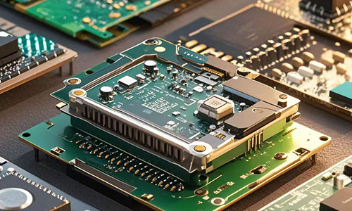
The 6-layer communication radio PCB is a high-performance PCB which designed for radio signal reception.
Technical Specifications
| Number of layers | 4 | Minimum line width and line spacing | 0.1/0.1mm |
| Board thickness | 2.0mm | Minimum aperture | 0.2 |
| Board material | S1000-2M | Surface treatment | 2” immersion gold |
| Copper thickness | 1oz inner layer 1OZ outer layer | Process points | impedance control + crimping hole |
| WHY US |
||||
 |
 |
 |
||
| Fast Delivery | High Quality | Diversified Customization | ||
| Factory | ||||
 |
 |
 |
||
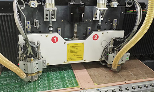
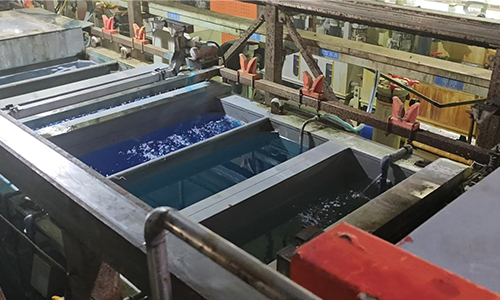
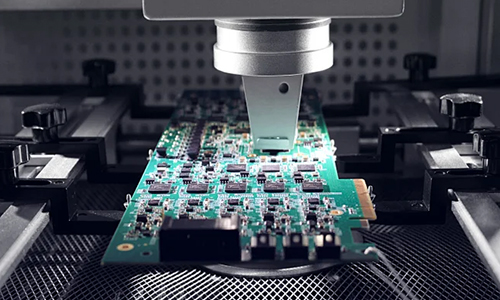
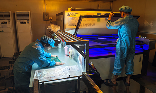
| Photoengraving Workshop | Drilling Machine | Electroplating Production Line | ||
| More Information | ||
| Strategic Partners | Application | Certificate |
FAQ
1.Q: When can I get a quotation after I provide Gerber, product process requirements?
A: Our sales staff will give you a quotation within 1 hour.
2.Q: How many employees do you have in your factory?
A: More than 500.
3.Q: How to solve the common overheating problems when using communication PCB boards?
A: The key is to introduce heat dissipation design and or choose high quality materials. For example: EMC, TUC, Rogers and other companies to provide the board.
4.Q: Can you provide samples?
A: We have the ability to quickly proof-sample PCB and provide comprehensive technical support.
 10-Layer High-Frequency & High-Speed Communication PCB
 6-layer 5G Communication System AC PCB
 12-layer Second-Generation Communication Receiver System Dedicated AC PCB
 14-layer Communication Receiving AC PCB
 4-Layer PCB for Small Optical Communication Instruments
 2-Layer Communication 5G Antenna PCB