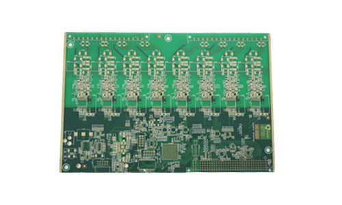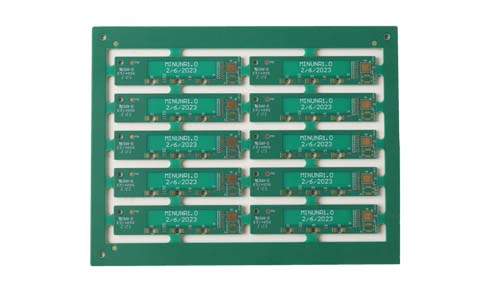
Our 4-layer communication router PCB circuit board is designed for high-performance network equipment to meet the needs of modern communication systems for high-speed data transmission and stability.
4-layer Communication PCB Product Introduction
 |
 |
1.Product Overview
Our 4-layer communication router PCB circuit board is designed for high-performance network equipment to meet the needs of modern communication systems for high-speed data transmission and stability. The circuit board uses high-quality materials and advanced manufacturing processes to ensure its reliability and performance in various complex environments.
2.Main Features
4-layer structure:
Adopting a 4-layer design, the power supply, ground and signal layers are reasonably laid out to effectively reduce signal interference, improve circuit performance, and are suitable for the complex wiring requirements of communication equipment.
High-frequency performance:
Adopting high-frequency FR-4 material, it has excellent electrical properties, supports high-speed signal transmission, and ensures data stability and integrity.
Good electromagnetic compatibility:
Electromagnetic interference (EMI) and signal integrity are fully considered during design, and a reasonable stacking structure and shielding design are adopted to ensure stable operation in various environments.
High-quality surface treatment:
Provide a variety of surface treatment options, such as ENIG (electroplating gold), HASL (hot air leveling), etc., to ensure good welding performance and corrosion resistance to meet different application requirements.
Precision manufacturing process:
Adopt advanced laser drilling and high-precision lithography technology to ensure high-precision processing of tiny apertures and thin line widths, and meet the needs of high-density wiring.
Comply with industry standards:
The product complies with industry standards such as IPC-A-600 and IPC-6012 to ensure the quality and reliability of PCBs, and is suitable for various high-end communication equipment.
3.Application Areas
Routers and switches: Suitable for various network routers and switches, providing stable network connections.
Wireless communication equipment: Widely used in wireless base stations, Wi-Fi devices, etc., supporting efficient data transmission.
Industrial automation: Used in industrial control systems and monitoring equipment to ensure real-time data transmission.
Consumer electronics: Suitable for communication products such as smart home devices and TV boxes.
4.Technical Specifications
| Number of layers | 4 | Minimum line width and line spacing | 0.1/0.1mm |
| Board thickness | 2.0mm | Minimum aperture | 0.2 |
| Board material | S1000-2M | Surface treatment | 2” immersion gold |
| Copper thickness | 1oz inner layer 1OZ outer layer | Process points | impedance control + crimping hole |
5.Production Capacity
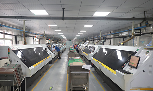
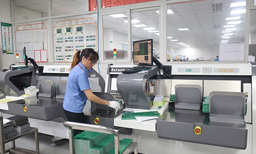
We have advanced production equipment and a professional technical team, with large-scale production capabilities to meet the diverse needs of customers. Support small-batch trial production and large-scale production, and timely delivery.
 |
 |
6.Customer Support
Provide comprehensive technical support and after-sales service to assist customers in solving various problems during the design, manufacturing and post-maintenance process to ensure the smooth progress of the project.
7.Conclusion
Our 4-layer communication router PCB circuit board is an ideal choice for your high-performance network equipment development. With its high reliability, excellent electrical performance and compliance with industry standards, it helps your products stand out in the highly competitive market. For more information or to obtain a quote, please feel free to contact us.
FAQ
Q: What is your minimum order quantity?
A: One piece is enough to place an order.
Q: When can I get a quotation after I provide Gerber, product process requirements?
A: Our sales staff will give you a quotation within 1 hour.
Q: Why do signals sometimes become incomplete in devices equipped with communication PCBs?
A: As design complexity increases, 5G devices may utilize HDI communication PCBs with finer traces and higher-density interconnections. When transmitting high-speed signals, these finer traces may lead to incomplete signals. If such issues occur, please contact our staff to make adjustments for your product.
Q: How many layers of HDI can your company produce?
A: We can produce from four layers of first order to high multi-layer arbitrary interconnect PCB circuit boards.
 10-Layer High-Frequency & High-Speed Communication PCB
 6-layer 5G Communication System AC PCB
 12-layer Second-Generation Communication Receiver System Dedicated AC PCB
 14-layer Communication Receiving AC PCB
 4-Layer PCB for Small Optical Communication Instruments
 2-Layer Communication 5G Antenna PCB