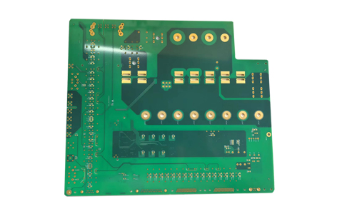
The 10-layer 5G communication PCB is high-performance designed for 5G communication equipment.
10-Layer 5G Communication PCB Product Introduction

1.Product Overview
The 10-layer 5G communication PCB is high-performance designed for 5G communication equipment.It adopts advanced multi-layer technology and combines high-frequency materials to meet the needs of high-speed data transmission and complex signal processing. widely used in 5G communication infrastructure such as base stations, antennas, routers, etc., supporting fast and stable wireless communication.
2.Product Features
1.High-frequency performance:
2.Adopt low dielectric constant (Dk) and low dielectric loss (Df) materials to ensure signal transmission stability and integrity under high-frequency conditions, meeting the high standards of 5G communication.
3.Multi-layer design:
4.10-layer structure provides higher wiring density and more complex circuit design capabilities, supporting effective management and processing of high-speed signals.
5.Excellent heat dissipation performance:
6.Heat dissipation management is taken into account in the design to ensure thermal stability under high-power operation and extend the service life of the equipment.
7.High reliability:
8.Strict production process and quality control are adopted to ensure the reliability of the product in harsh environments and adapt to various application scenarios.
9.Strong anti-interference ability:
10.Adopt good electromagnetic shielding design to reduce the impact of external interference on the signal and improve the communication quality.
11.Lightweight and compact design:
12.The design focuses on lightweight and compactness, which is easy to integrate into various communication equipment, and improves the portability and installation flexibility of the overall equipment.
3.Technical Specifications
| Number of layers | 10 layers | Ink color | green oil white text |
| Material | FR-4, SY1000-2 | Minimum line width/line spacing | 0.075mm/0.075mm |
| Thickness | 2.0mm | Is there solder mask: | yes |
| Copper thickness | inner 0.1 outer layer 1OZ | Surface treatment | immersion gold + electro-thick gold 30 wheat |
4.Application Areas
Base station equipment: RF modules and signal processing units supporting 5G base stations.
Antenna system: used for high-frequency signal transmission and reception of 5G antennas.
Network equipment: such as routers, switches, etc., supporting high-speed data transmission.
IoT devices: provide a stable communication foundation for various 5G IoT applications.
5.Production Process
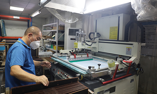
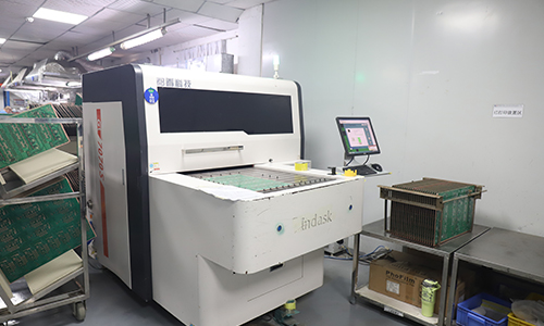
Precision etching and laser drilling: ensure the accuracy of the circuit pattern to meet the requirements of high-density interconnection (HDI).
Multi-layer lamination technology: combine different layers of materials through high temperature and high pressure processes to ensure electrical performance and mechanical strength.
Surface treatment: provide a variety of surface treatment options, such as metallization (ENIG, HASL, etc.) to improve welding reliability and corrosion resistance.
 |
 |
6.Conclusion
The 10-layer 5G communication PCB has become an indispensable and important part of 5G communication equipment with its excellent performance, reliability and broad application prospects. Whether in signal transmission, thermal management or anti-interference ability, it has shown significant advantages, promoting the widespread application and development of 5G technology.
FAQ:
1.Q: How far is your factory from the nearest airport?
A: About 30 kilometers
2.Q: What is your minimum order quantity?
A: One piece is enough to place an order.
3.Q: When can I get a quotation after I provide Gerber, product process requirements?
A: Our sales staff will give you a quotation within 1 hour.
4.Q: How to solve the common overheating problems when using communication PCB boards?
A: The key is to introduce heat dissipation design and or choose high quality materials. For example: EMC, TUC, Rogers and other companies to provide the board.
5.Q: How to avoid high-frequency and high-speed PCB circuit board common signal interference?
A: The need to optimize the PCB layout and reasonable planning of the ground to reduce the impact of interference.
6.Q: Do you have laser drilling machines?
A: We have the most advanced laser drilling machine in the world.
7.Q: Can your company manufacture impedance boards and crimp hole circuit boards?
A: We can produce impedance PCBs, and the same product can be made with multiple impedance values. We can also manufacture precision holes for crimp holes.
 10-Layer High-Frequency & High-Speed Communication PCB
 6-layer 5G Communication System AC PCB
 12-layer Second-Generation Communication Receiver System Dedicated AC PCB
 14-layer Communication Receiving AC PCB
 4-Layer PCB for Small Optical Communication Instruments
 2-Layer Communication 5G Antenna PCB