
Let's continue to learn about the main difficulties of IC substrates manufacturing process:
1. Solder mask: In the manufacturing process of IC substrates, creating a solder mask is crucial. The surface layer of IC substrates is very thin, typically not exceeding 10 micrometers, and the dimensional tolerance between the solder mask and the pad must be controlled within 15 micrometers. This requires the application of solder mask on IC substrates to be more delicate than on PCBs. Therefore, we must use specialized techniques, equipment, and procedures for solder mask printing and through-hole filling to ensure precision and quality.
2. Surface treatment: Surface treatment of IC substrates includes polishing and smoothing processes. Although this step may not be as complex as other steps in the manufacturing process, it still requires great care. We must focus on ensuring the uniformity of the IC substrate surface to improve the reliability of soldering and circuit performance. Common surface treatment techniques include Electroless Nickel Immersion Gold (ENIG) or Electroless Nickel Palladium Immersion Gold (ENEPIG).
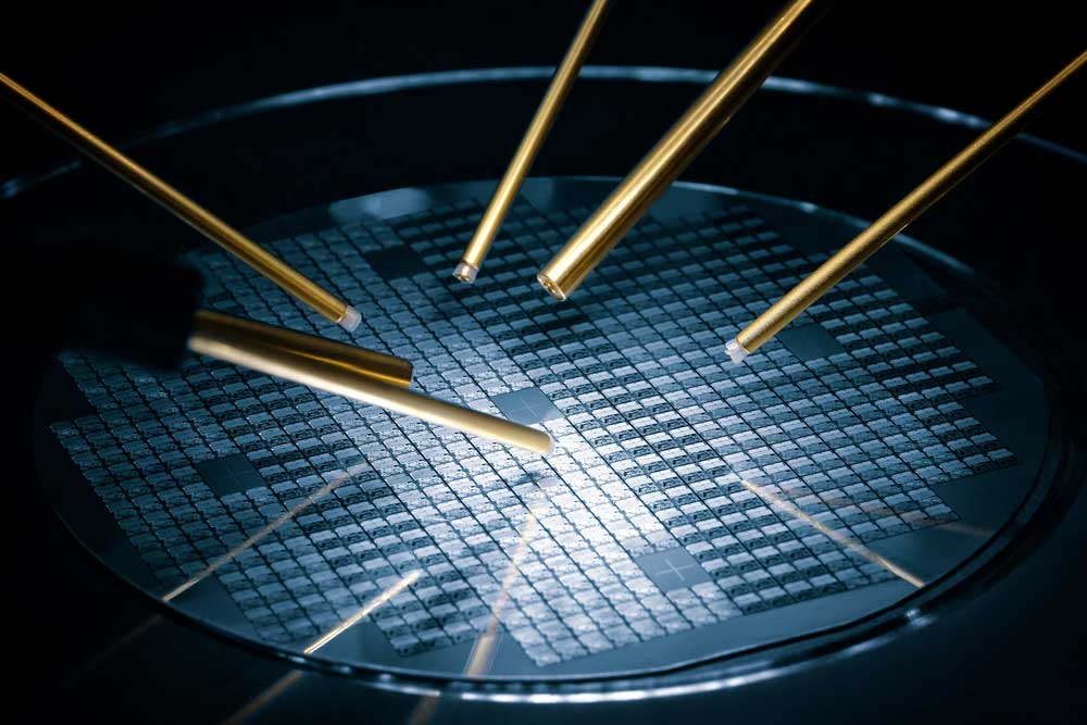
3. Inspection capabilities and product reliability testing techniques: In the final stage of the manufacturing process, we particularly need to test and ensure the normal use of the entire IC substrate through sampling and various testing techniques, such as flying probe testing, test fixture testing, and manual inspection. These tests are crucial for verifying the electrical performance and mechanical integrity of the substrate.
The above is a detailed explanation of IC substrates. If you are also interested in IC substrates and want to customize an IC substrate product, please feel free to contact our sales staff and place an order.


