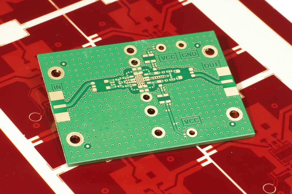

The manufacturing process of IC substrates is highly complex, leading to numerous challenges. Here are some of the main difficulties:
1. Substrate manufacturing: IC substrates are extremely fragile and prone to deformation due to their fine dimensions and high consistency. This fragility is particularly evident in substrates with widths less than 0.2mm. To control and prevent substrate deformation, we need to optimize lamination parameters and layer positioning techniques. At the same time, meticulous management of the material shrinkage process is key to ensuring optimal performance.
2. Microvia fabrication technology: This technology includes multiple steps such as laser drilling, electroplating through-holes, conformal masking, and copper panel filling. As integrated circuits and their substrates continue to miniaturize, the precise application of these technologies becomes particularly challenging. However, by employing blind and conformal masks, we can simplify the laser drilling process and improve manufacturing precision.
3. Patterning and copper plating technology: For complex external patterns, especially those with small dimensions, patterning and copper plating technologies face significant challenges. This technology requires precise circuit control and compensation, uniform copper plating thickness, and the ability to manufacture fine lines. Additionally, the accurate application of bonding techniques is key to achieving high-quality substrates.
We will continue to discuss other manufacturing challenges in the next article.