4-layer PCB circuit board with IC carrier is a high-performance printed circuit board designed for complex electronic equipment and widely used in communications, consumer electronics, automotive electronics and industrial control.
4-Layers PCB With IC Carrier Product Introduction
1.Product Overview
4-layer PCB circuit board with IC carrier is a high-performance printed circuit board designed for complex electronic equipment and widely used in communications, consumer electronics, automotive electronics and industrial control. By integrating IC carrier on PCB, higher integration and better signal transmission performance can be achieved.
2.Main Features
Multi-layer structure:
4-layer design provides larger wiring space, which can effectively reduce signal interference and electromagnetic interference (EMI), and improve the stability and reliability of the circuit.
High-density wiring:
Suitable for high-density component layout, it can realize complex circuit design in a limited space, and meet the needs of modern electronic equipment for miniaturization and high performance.
Excellent signal integrity:
Through reasonable stacking structure and wiring design, it can effectively reduce signal delay and reflection, and ensure the transmission quality of high-frequency signals.
Integrated IC carrier:
Integrating IC carrier on PCB can achieve higher functional integration, simplify circuit design, and improve the overall performance of the system.
Good heat dissipation performance:
High thermal conductivity materials and reasonable layout design can effectively dissipate heat and ensure the stability of IC and other components during operation.
3.Technical Parameters
| Number of layers | 4 | Minimum line width and line spacing | 0.3/0.3MM |
| Board thickness | 0.6mm | Minimum aperture | 0.3 |
| Board material | FR-4 SY1000-2 | Solder mask | green oil and white text |
| Copper thickness | 1OZ | Surface treatment | immersion gold |
| Process points: | no lead residue + high temperature glue | / | / |
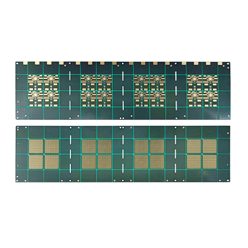
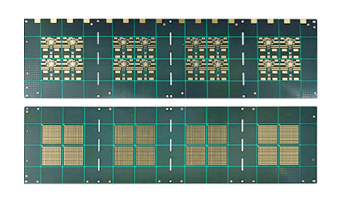
4.Structure
A 4-layer PCB circuit board with IC carrier usually consists of the following parts:
Top layer (Layer 1): mainly used for signal input and output, arranging important components and connections.
Inner layer 1 (Layer 2): used for the distribution of power and ground lines, providing stable power supply and good grounding.
Inner layer 2 (Layer 3): used for signal transmission, optimizing signal integrity and reducing interference.
Bottom layer (Layer 4): used for signal output and connection, usually with fewer components arranged.
5.Application Fields
Communication equipment: such as mobile phones, routers and base stations.
Consumer electronics: such as smart home devices, tablets and game consoles.
Automotive electronics: such as in-car entertainment systems, navigation equipment and sensors.
Industrial control: such as PLC, automation equipment and monitoring systems.
 |
 |
6.Conclusion
The 4-layer PCB circuit board with IC carrier has become an indispensable basic component in modern electronic devices due to its excellent signal integrity, high-density wiring and good heat dissipation performance. With the continuous advancement of electronic technology and the increase in market demand, the application of this PCB will continue to expand, providing more efficient and reliable solutions for various industries.
FAQ
Q: Do you have an office address that could be visited?
A: Our office address is Tianyue Building, Bao 'an District, Shenzhen.
Q: Will you attend the exhibition to show your products?
A: We are planning on it.
Q: What aspects are included in the testing control of IC carrier boards?
A: The testing control of IC carrier boards includes:
Testing equipment: Testing multi-layer PCB requires the use of professional testing equipment, and the appropriate testing equipment should be chosen to ensure the accuracy and reliability of the testing.
Problem localization: For produced PCB with issues, problems can be localized and solved by comparing and isolating defective components, testing integrated circuits, detecting power supplies, and other methods.
Q: Do you have your own surface treatment production line?
A: Sure, we have the surface treatment line.