The 4-layer mobile phone dedicated IC carrier board PCB is a high-performance printed circuit board designed for small electronic devices such as mobile phones.
1.Product Overview
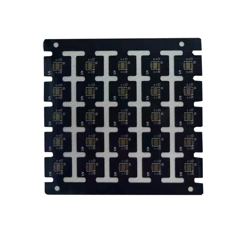
The 4-layer mobile phone dedicated IC carrier board PCB is a high-performance printed circuit board designed for small electronic devices such as mobile phones. It uses black solder mask and electroplating technology, combined with HDI (high-density interconnection) technology, to achieve a perfect combination of miniaturization and high performance. With its excellent electrical performance and mechanical strength, this PCB provides stable and reliable circuit connections for mobile phones and other devices.
2.Product Features
1. High-density interconnection (HDI process): Through the HDI process, finer lines and higher circuit density are achieved, which is suitable for the space limitations of small electronic devices.
2. Electroplating technology: The electroplating technology is used to improve welding reliability and oxidation resistance, and extend the service life of the product.
3. Black solder mask: The black solder mask provides excellent visual effects and insulation performance, protecting the circuit from external interference.
3.Technical Specifications
| Number of layers | 4 layers | Board thickness | 1.0mm |
| Solder mask color | Black | Copper foil thickness | 1OZ |
| Surface treatment process | Electroplating process | Minimum line width/line spacing | 0.1mm/0.1mm |
| Board type | High TG FR-4 material, polyimide material | Thermal expansion coefficient | 13-17ppm/°C |
| Packaging method | 1Panel=25Pcs | / | / |
4.Application
1. Mobile phones: As mobile phone motherboard, it supports high-speed data processing and signal transmission.
2. Wearable electronic devices: In smart watches and other wearable devices, it is used as the core control board to achieve miniaturization and high performance.
5.Production Process
Lamination: Bonding the layers of board and copper foil together through high temperature and high pressure.
Laser drilling: Use laser drilling technology to accurately drill the required hole diameter to achieve high-precision hole position.
Solder mask: Apply black solder mask ink, and form the solder mask by screen printing and UV curing.
Electroplating: A layer of nickel-gold is deposited on the surface of the copper layer to improve welding performance and anti-oxidation ability.
6.Summary
The 4-layer mobile phone dedicated IC carrier PCB has become the preferred choice for high-performance PCBs in small electronic devices with its HDI process and electroplating surface treatment. It not only meets the needs of miniaturization, but also provides excellent electrical performance and environmental protection characteristics through the black solder mask layer. This PCB is widely used in the field of mobile phones and wearable devices, and is a reliable choice for your electronic product design and manufacturing.
FAQ
1.Q: How many employees do you have in your factory?
A: More than 500.
2.Q: Are the materials you use environmentally friendly?
A: The materials we use are in accordance with ROHS standard and IPC-4101 standard.
3.Q: How does the IC substrate achieve signal transmission connections?
A: IC substrates are positioned between chips and PCBs to achieve signal transmission connections, while also providing protection and support for the chips and forming a heat dissipation channel, so that the packaged chips achieve the required dimensions.
4.Q: Can your company manufacture impedance boards and crimp hole circuit boards?
A: We can produce impedance PCBs, and the same product can be made with multiple impedance values. We can also manufacture precision holes for crimp holes.