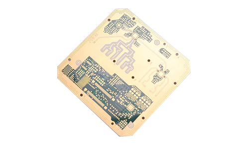
This circuit board has superior electrical performance, low loss and good thermal stability, and is widely used in wireless communication, satellite communication, radar and other high-frequency electronic equipment.
5G Communication High Frequency Board Product Introduction

1.Product Overview
10-layer high-frequency board for communication is a multi-layer printed circuit board (PCB) designed for high-frequency communication applications, usually using high-performance materials (such as RO4003C, RO4350B, etc.). This circuit board has superior electrical performance, low loss and good thermal stability, and is widely used in wireless communication, satellite communication, radar and other high-frequency electronic equipment.
2.Product Features
High-frequency performance
Low dielectric constant (Dk) and low dielectric loss (Df) ensure the effective transmission of high-frequency signals.
Provide excellent signal integrity, suitable for high-speed data transmission.
Multi-layer structure
10-layer design provides abundant wiring space, supports complex circuit design and separation of multiple signal layers.
Suitable for high-density interconnect (HDI) design to meet the needs of modern electronic products.
Excellent thermal management
High thermal conductivity materials can effectively dissipate heat and adapt to high-power and high-frequency applications.
Improve the reliability and stability of the circuit board.
Mechanical strength
With good mechanical strength and durability, it is suitable for complex circuit layout and environment.
Good processability
Easy to process and manufacture, suitable for mass production and fast delivery.
3.Application Areas
Wireless communication: such as base stations, mobile communication equipment, etc.
Satellite communication: stable transmission of high-frequency signals.
Radar system: high-precision signal processing and transmission.
IoT equipment: support high-frequency data transmission and connection.
 |
 |
4.Technical Parameters
| Number of layers | 10 layers | Process | immersion gold |
| Board thickness | 1.6MM | Minimum drilling | 0.1mm |
| Material | Rogers | Minimum line width | 0.3mm |
| Solder mask color | green oil and white characters | Minimum line spacing | 0.3mm |
5.Conclusion
The 10-layer high-frequency board for communication is an ideal choice in the field of high-frequency communication. With its excellent electrical performance, thermal stability and multi-layer design, it can meet the strict requirements of modern communication equipment for high-performance circuit boards. Whether in wireless communication, satellite communication or other high-frequency applications, this high-frequency board can provide reliable solutions.
FAQ:
Q: What files are used in PCB production?
A: PCB production requires Gerber files and PCB manufacturing specifications, such as the required substrate material, finished thickness, copper layer thickness, solder mask color, and design layout requirements.
Q: When can I get a quotation after I provide Gerber, product process requirements?
A: Our sales staff will give you a quotation within 1 hour.
Q: Does chemical de-fluxing work on PTFE materials?
A: PTFE resin is highly inert, and chemical de-fluxing solutions have no effect on PTFE resin. However, for PTFE resin boards mixed with a large amount of ceramic fillers, chemical de-fluxing solutions can attack the ceramic fillers, thereby affecting the electrical properties of the board. Therefore, chemical de-fluxing is not recommended for PTFE boards with this structure.
Q: Can you provide samples?
A: We have the ability to quickly proof-sample PCB and provide comprehensive technical support.