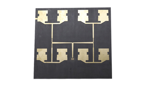
Double-sided 5G antenna PCB circuit board is a high-performance printed circuit board designed for 5G communication technology.
Double-Sided Antenna PCB Product Introduction

1.Product Overview
Double-sided 5G antenna PCB circuit board is a high-performance printed circuit board designed for 5G communication technology. It has the characteristics of double-sided wiring and can meet the needs of 5G network for high-frequency and high-speed signal transmission. This product is widely used in 5G base stations, smart phones, IoT devices and other wireless communication devices.
2.Product Features
1.High-frequency performance
2.The design supports a frequency range of up to 30GHz, ensuring stable signal transmission within the 5G frequency band.
3.Double-sided wiring design
4.Circuit wiring can be performed on both sides, providing greater design flexibility and higher circuit density.
5.High-quality materials
6.Adopt low dielectric constant and low-loss substrates (such as PTFE, FR-4, etc.) to effectively reduce signal attenuation and reflection.
7.High heat dissipation performance
8.Design a reasonable heat dissipation structure to ensure stability during high-power operation and extend the service life of the equipment.
9.Precision manufacturing process
10.Use advanced manufacturing technology to ensure high line accuracy and suitable for complex circuit design.
Application Areas
5G base station
Antenna system for 5G base stations, supporting high-speed data transmission and wide coverage.
Smartphones
Integrated into 5G smartphones to provide stable network connections.
devices
Various 5G IoT sensors and controllers to enhance the communication capabilities of devices.
Automotive electronics
In-vehicle 5G communication modules to support autonomous driving and Internet of Vehicles applications.
3.Technical Parameters
| Number of layers | 2L | Minimum line width/line spacing | 0.12mm |
| Board thickness | 0.6mm | Outer copper thickness | 1OZ |
| Board material | Teflon polytetrafluoroethylene | Surface treatment | immersion gold |
| Minimum aperture | 0.8mm | / | / |
4.Design and Manufacturing Process
1.Demand analysis
Communicate with customers to understand product requirements and technical specifications to ensure that the design meets 5G standards.
2.Circuit design
Use professional software for circuit design to optimize signal paths and reduce interference.
3.PCB layout
Perform double-sided layout to reasonably arrange the positions of antennas and other circuit components.
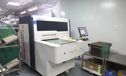
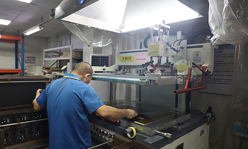
4.Manufacturing
Use high-precision equipment for PCB production to ensure product quality and performance.
5.Testing and Verification
Perform strict electrical performance tests and environmental adaptability tests on finished products to ensure that they meet design requirements.
 |
 |
5.Summary
Double-sided 5G antenna PCB circuit boards are key components for realizing 5G communication technology. With their superior performance and broad application prospects, they have become an indispensable part of modern wireless communication equipment. We are committed to providing customers with high-quality products and professional technical support to meet the needs of the evolving 5G market.
FAQ
Q: Are the materials you use environmentally friendly?
A: The materials we use are in accordance with ROHS standard and IPC-4101 standard.
Q: How far is your factory from the nearest airport?
A: About 30 kilometers
Q: How to avoid high-frequency and high-speed PCB circuit board common signal interference?
A: The need to optimize the PCB layout and reasonable planning of the ground to reduce the impact of interference.
Q: Can your company manufacture impedance boards and crimp hole circuit boards?
A: We can produce impedance PCBs, and the same product can be made with multiple impedance values. We can also manufacture precision holes for crimp holes.