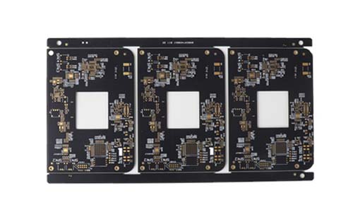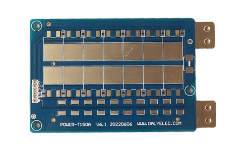
Our 8-layer first-order HDI (high-density interconnect) PCB circuit board is designed for high-performance electronic devices, especially for applications with extremely high requirements for signal integrity and miniaturization.
8-layer First Order PCB Product Introduction
 |
 |
1.Product Overview
Our 8-layer first-order HDI (high-density interconnect) PCB circuit board is designed for high-performance electronic devices, especially for applications with extremely high requirements for signal integrity and miniaturization. This circuit board adopts advanced manufacturing technology and high-quality materials to provide excellent electrical performance and reliability to meet the needs of modern electronic products.
2.Main Features
8-layer structure:
Adopting 8-layer design, it provides abundant wiring space, supports complex circuits and multi-functional integration, and is suitable for the application of high-density components.
First-order HDI technology:
The first-order HDI structure has micro-blind and micro-buried hole designs, which can achieve higher wiring density and shorter signal paths, and improve signal transmission speed and stability.
High-quality materials:
Adopting high-performance FR-4 or other high-frequency materials, it has excellent insulation performance and thermal stability to ensure reliability for long-term use.
Precision manufacturing process:
Adopting laser drilling and high-precision lithography technology to ensure high-precision processing of tiny apertures and fine line widths, adapting to the needs of high-density wiring.
Good electromagnetic compatibility:
Electromagnetic interference (EMI) and signal integrity are fully considered during design, and reasonable stacking structure and shielding design are used to ensure stable operation of the circuit in various environments.
Multiple surface treatment options:
Provide a variety of surface treatment methods, such as ENIG (electroplating gold), OSP (organic coating protection), etc., to ensure welding performance and corrosion resistance, and adapt to different application requirements.
Compliance with industry standards:
Products comply with industry standards such as IPC-A-600, IPC-6012, etc., to ensure the quality and reliability of PCBs, and are suitable for various high-end electronic devices.
3.Application Areas
Smart phones and mobile devices: meet the design requirements of high integration and thinness.
Medical equipment: suitable for high-precision medical monitoring equipment and diagnostic instruments.
Automotive electronics: support advanced automotive electronic systems such as ADAS (advanced driver assistance system).
Consumer electronics: widely used in high-end audio, smart home devices, etc.
4.Technical Specifications
| Number of layers | 8 | Minimum line width and line spacing | 0.075/0.075mm |
| Board thickness | 1.03mm | Minimum aperture | 0.1 |
| Board material | S1000-2M | Surface treatment | 2” immersion gold |
| Copper thickness | 0.5 inner layer, 1OZ outer layer | Process points | HDI first order + countersunk hole + BGA size 0.2mm |
5.Production capacity
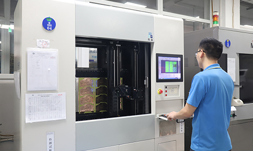
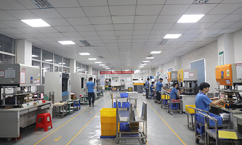
We have advanced production equipment and a professional technical team, with large-scale production capabilities to meet the diverse needs of customers. Support small batch trial production and large batch production, and timely delivery.
 |
 |
6.Customer Support
Provide comprehensive technical support and after-sales service to assist customers in solving various problems during the design, manufacturing and post-maintenance process to ensure the smooth progress of the project.
7.Conclusion
Our 8-layer first-order HDI PCB circuit board is an ideal choice for your high-performance electronic device development. With its high density, high reliability and compliance with industry standards, it helps your products stand out in the highly competitive market. For more information or to obtain a quote, please feel free to contact us.
FAQ
Q: How many employees do you have in your factory?
A: More than 500.
Q: Are the materials you use environmentally friendly?
A: The materials we use are in accordance with ROHS standard and IPC-4101 standard.
Q: What problems can be caused by inaccurate PCB design in mobile phones?
A: If the circuit design lacks a rational layout, it may lead to signal interference and unstable transmission, thereby affecting the performance of the entire phone. Therefore, we need to fully consider the position of each component and the rationality of the wiring during the PCB design phase.
Q: Can your company manufacture impedance boards and crimp hole circuit boards?
A: We can produce impedance PCBs, and the same product can be made with multiple impedance values. We can also manufacture precision holes for crimp holes.