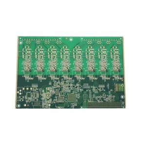
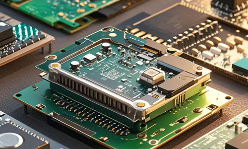
Our 4-layer communication PCB is designed for high-performance network equipment to meet the needs of modern communication systems for high-speed data transmission and stability.
Technical Specifications
| Number of layers | 4 | Minimum line width and line spacing | 0.1/0.1mm |
| Board thickness | 2.0mm | Minimum aperture | 0.2 |
| Board material | S1000-2M | Surface treatment | 2” immersion gold |
| Copper thickness | 1oz inner layer 1OZ outer layer | Process points | impedance control + crimping hole |
| WHY US |
||||
 |
 |
 |
||
| Fast Delivery | High Quality | Diversified Customization | ||
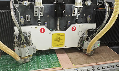
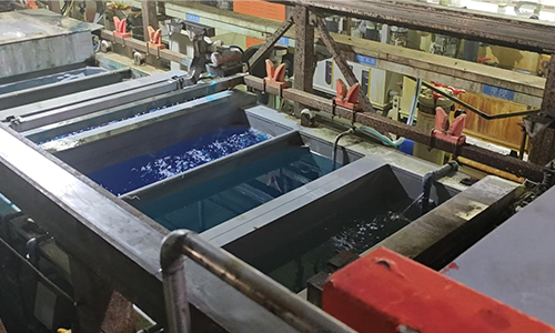
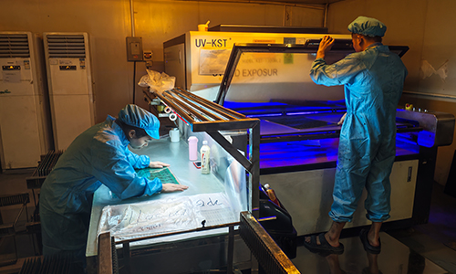
| Factory | ||||
 |
 |
 |
||
| Photoengraving Workshop | Drilling Machine | Electroplating Production Line | ||
| More Information | ||
| Strategic Partners | Application | Certificate |
FAQ
1.Q: What is your minimum order quantity?
A: One piece is enough to place an order.
2.Q: When can I get a quotation after I provide Gerber, product process requirements?
A: Our sales staff will give you a quotation within 1 hour.
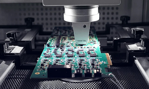
3.Q: Why do signals sometimes become incomplete in devices equipped with communication PCB?
A: As design complexity increases, 5G devices may utilize HDI communication PCB with finer traces and higher-density interconnections. When transmitting high-speed signals, these finer traces may lead to incomplete signals. If such issues occur, please contact our staff to make adjustments for your product.
4.Q: How many layers of HDI can your company produce?
A: We can produce from four layers of first order to high multi-layer arbitrary interconnect PCB circuit boards.