
The next two types of lamination structures to be presented are the "N+N" structure and the any-layer interconnect structure.
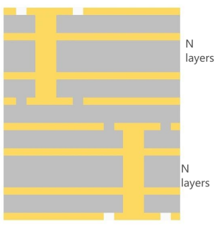
The N+N lamination structure, as shown in the cover diagram, is composed of two large multi-layer boards. Although the N+N lamination may not have blind holes, due to the special process and strict alignment requirements, the actual manufacturing difficulty is not less than that of HDI PCB.

Any-layer interconnect structure, in other words, means that any layer can be connected.
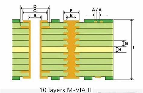
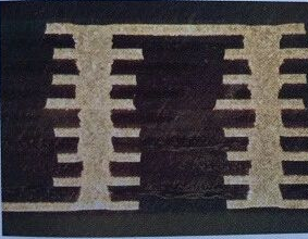
As shown in the figure above, many blind via are stacked together to form an any-layer interconnect structure.

From the cross-section in the picture above, it can also be seen that stacking each layer together to form straight lines is also a challenge, so the any-layer process is also a test of the accuracy of the factory's equipment; the lines made in this way will definitely be very dense and fine.
In summary, despite facing many challenges, HDI lamination design has become a key part of high-end electronic products. From smartphones to wearable devices, from high-performance computers to advanced communication systems, HDI technology is playing a key role. With the continuous advancement of technology and the increasing demands of consumers, we have reason to believe that HDI lamination technology will continue to lead the trend of innovation in the field of electronics manufacturing. Sanxis will also follow the latest technology trends, make good use of HDI lamination technology, and create better PCB products for our customers.