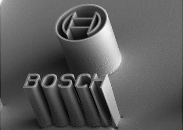

In the production and manufacturing of PCB, the "Bosch process" is a deep silicon etching technology, particularly suitable for applications such as Through-Silicon Vias (TSV) and Micro-Electro-Mechanical Systems (MEMS), which require the etching of deep holes or slots in silicon wafers. The Bosch process ensures the steepness of the sidewalls by alternating etching and passivation gases, achieving high aspect ratio structure etching.
First, let’s learn about the name and background of Bosch technique.
This process was initially developed by Robert Bosch GmbH to meet the demand for high aspect ratio silicon structures in micro-electromechanical systems (MEMS) products. Due to its advantages in realizing complex three-dimensional silicon structures, the Bosch process has quickly gained widespread application in the semiconductor manufacturing field.
In the next article, we will explore the raw materials required for the Bosch process, mainly the etching gas SF6 and the passivation gas C4F8. These gases are used alternately, and through a periodic "etching-passivation-etching" process, etching proceeds only in the depth direction, thus achieving high aspect ratio and steep sidewall silicon structure etching.