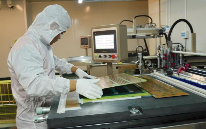

Workers are Working at The Solder Masking Workbench.
Solder mask is an essential step in the PCB manufacturing process. How can the principle of solder mask be scientifically explained? Today, we will explain from the following four points:
1.Physical blocking. The solder mask layer is usually an insulating material, such as solder mask ink. It covers the conductors and pads of the PCB, forming a physical barrier to prevent solder from adhering to areas where soldering is not needed.
2.Utilize surface tension. During soldering, solder has surface tension. The solder mask layer can change its surface tension, making solder more likely to gather in areas where soldering is needed and reducing adhesion in other areas.
3.Chemical reaction. The material of the solder mask layer may react chemically with solder to form a stable compound, enhancing the solder mask effect.
4.Thermal stability. The solder mask layer needs to not melt or decompose under high soldering temperatures to maintain the solder mask function and ensure that the protected area is not affected by solder during the soldering process, safeguarding the stable operation of the circuit board.