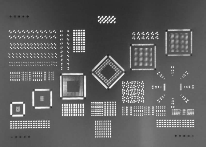

Today we will learn about some special SMT PCB components and the Requirements for the shape and size of the apertures on the glue printing stencil.
1. Aperture design for certain special SMT components:
1) CHIP components: For CHIP components larger than 0603, effective measures are taken to prevent the formation of solder balls.
2) SOT89 components: Due to the large pad size and small pad spacing, solder balls and other quality issues in welding may easily occur.
3) SOT252 components: Since one of the pads of the SOT252 is quite large, it is prone to solder balls and may cause shift due to the tension during reflow soldering.
4) IC components: A. For standard pad design, ICs with a PITCH of 0.65mm or greater, the aperture width is 90% of the pad width, with the length remaining unchanged. B. For standard pad design, ICs with a PITCH of less than 0.05mm are prone to bridging due to their small PITCH. The stencil aperture length remains unchanged, the aperture width is 0.5 times the PITCH, and the aperture width is 0.25mm.
5) Other situations: When one pad is excessively large, typically with one side greater than 4mm and the other side not less than 2.5mm, to prevent the formation of solder balls and shifts caused by tension, it is recommended to use a grid line division method for the stencil aperture. The grid line width is 0.5mm, and the grid size is 2mm, which can be evenly divided according to the size of the pad.
2. Requirements for the shape and size of the apertures on the glue printing stencil:
For simple PCB assemblies using the glue process, point gluing is preferred. CHIP, MELF, and SOT components are glued through the stencil, while ICs should use point gluing to avoid scraping the glue off the stencil. Here, only the recommended aperture sizes and shapes for CHIP, MELF, and SOT glue printing stencils are provided.
1) The diagonal of the stencil must have two diagonal positioning holes, and the FIDUCIAL MARK points are used for opening.
2) The apertures are all in a rectangular shape. Inspection methods:
(1) Visually inspect the apertures to ensure they are centered and the mesh is flat.
(2) Check the correctness of the stencil apertures with a physical PCB.
(3) Use a high-magnification video microscope with a scale to inspect the length and width of the stencil apertures, as well as the smoothness of the hole walls and the surface of the stencil sheet.
(4) The thickness of the stencil sheet is verified by measuring the thickness of the solder paste after printing, i.e., result verification.
We will learn other knowledge about PCB SMT stencil in next news article.