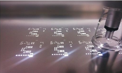

Let’s continue to learn about the design requirements for the fabrication of SMT stencils.
The general factory can accept the following three types of document formats for stencil making:
1. Design files generated by PCB design software, with the suffix name often being "*.PCB".
2. GERBER files or CAM files exported from PCB files.
3. CAD files, with the suffix name being "*.DWG" or "*.DXF".
In addition, the materials we require from customers for making templates generally include the following layers:
1. The circuit layer of the PCB board (containing the complete materials for making the template).
2. The silkscreen layer of the PCB board (to confirm the component type and printing side).
3. The pick-and-place layer of the PCB board (used for the aperture layer of the template).
4. The solder mask layer of the PCB board (used to confirm the position of the exposed pads on the PCB board).
5. The drill layer of the PCB board (used to confirm the position of through-hole components and vias to be avoided).
The aperture design of the stencil should consider the demolding of the solder paste, which is mainly determined by the following three factors:
1) The aspect ratio/area ratio of the aperture: The aspect ratio is the ratio of the aperture width to the stencil thickness. The area ratio is the ratio of the aperture area to the cross-sectional area of the hole wall. To achieve a good demolding effect, the aspect ratio should be greater than 1.5, and the area ratio should be greater than 0.66.
When designing the apertures for the stencil, one should not blindly pursue the aspect ratio or area ratio while neglecting other process issues, such as bridging or excess solder. Additionally, for chip components larger than 0603 (1608), we should consider more on how to prevent solder balls.
2) The geometric shape of the aperture sidewalls: The lower aperture should be 0.01mm or 0.02mm wider than the upper aperture, that is, the aperture should be in a inverted conical shape, which facilitates the smooth release of the solder paste and reduces the number of stencil cleanings. Under normal circumstances, the aperture size and shape of the SMT stencil are the same as the pad, and are opened in a 1:1 manner. Under special circumstances, some special SMT components have specific regulations for the aperture size and shape of their stencils.
3) The surface finish and smoothness of the hole walls: Especially for QFP and CSP with a pitch less than 0.5mm, the stencil manufacturer is required to perform electro-polishing during the production process.
We will learn other knowledge about PCB SMT stencil in next news article.