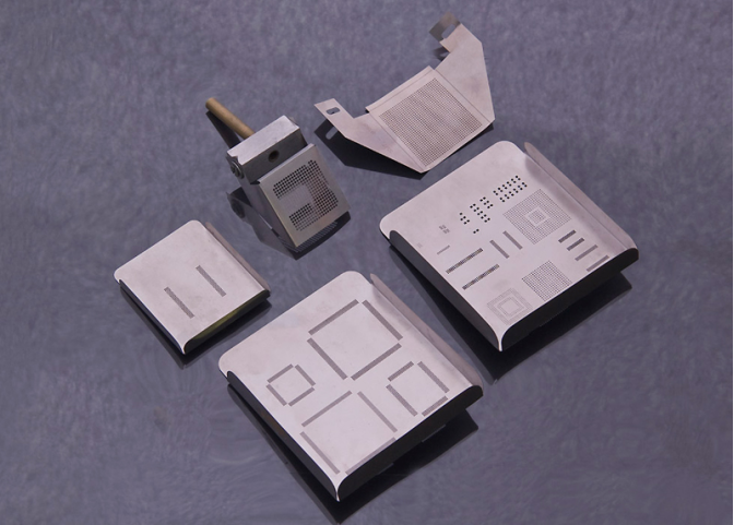

Now let’s learn about the design requirements for the fabrication of SMT stencils.
1. General Principle: The design of the stencil shall be in accordance with the IPC-7525 stencil design guidelines, with the main purpose being to ensure that the solder paste can smoothly release from the stencil apertures onto the PCB pads.
The design of the SMT stencil mainly includes the following eight elements:
Data format, Process method requirements, Material requirements, Material thickness requirements, Frame requirements, Printing format requirements, Aperture requirements, and Other process needs.
2. Stencil (SMT template) aperture design tips:
1) For fine-pitch ICs/QFPs, to prevent stress concentration, it is best to have rounded corners on both ends; the same applies to BGAs and 0400201 components with square apertures.
2) For chip components, the anti-solder ball design is best chosen as a concave opening method, which can effectively prevent the occurrence of component tombstoning.
3) In stencil design, the aperture width should ensure that at least 4 of the largest solder balls can pass through smoothly.
3. Documentation preparation before SMT stencil template design
Some necessary documentation must be prepared before the stencil template design:
- If there is a PCB Layout, it is required to provide the following according to the placement plan:
(1) The pad layer (PADS) where the pick-and-place components (SMDs) with Mark are located;
(2) The silkscreen layer (SILK) corresponding to the pads of the pick-and-place components;
(3) The top layer (TOP) containing the PCB border;
(4) If it is a panelized board, the panelized board diagram must be provided.
- If there is no PCB Layout, a PCB prototype or film negatives or scanned images at a 1:1 scale with the PCB prototype is required, which specifically includes:
(1) The setting of Mark, PCB outline data, and the pad positions of the pick-and-place components, etc. If it is a panelized board, the panelized style must be provided;
(2) The printing surface must be indicated.
More information will be shown in the next new.