
Today we will continue to learn about the third method of manufacturing PCB SMT stencils: Electroforming.
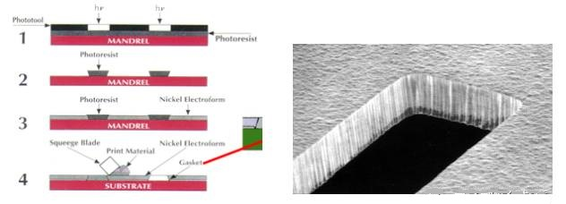
1. Principle Explanation: Electroforming is the most complex stencil manufacturing technology, which uses an electroplating process to build up a nickel layer to the required thickness around a pre-made core, resulting in precise dimensions that do not require post-processing to compensate for hole size and hole wall surface finish.
2. Process Flow: Apply a photosensitive film to the base board → Fabricate the core axis → Electroplate nickel around the core axis to form the stencil sheet → Strip and clean → Inspect → Tension the mesh → Package
3. Features: The hole walls are smooth, making it particularly suitable for the production of ultra-fine pitch stencils.
4. Disadvantages: The process is difficult to control, the production process is polluting and not environmentally friendly; the production cycle is long and the cost is high.
Electroformed stencils have smooth hole walls and a trapezoidal structure, which provide the best release of solder paste. They offer excellent printing performance for micro BGA, ultra-fine pitch QFP, and small component sizes such as 0201 and 01005. Moreover, due to the inherent characteristics of the electroforming process, a slightly raised annular projection is formed at the edge of the hole, which acts as a "sealing ring" during solder paste printing. This sealing ring helps the stencil to closely adhere to the pad or solder resist, preventing solder paste from leaking to the side of the pad. Of course, the cost of stencils made with this process is also the highest.
In the next article, we will introduce the Hybrid process method in PCB SMT stencil.