
Today, we will discuss how to choose the thickness and design the apertures when using SMT stencils.
Selection of SMT Stencil Thickness and Aperture Design
Controlling the amount of solder paste during the SMT printing process is one of the critical factors in SMT process quality control. The amount of solder paste is directly related to the thickness of the stencil template and the shape and size of the apertures (the speed of the squeegee and the pressure applied also have a certain impact); the thickness of the template determines the thickness of the solder paste pattern (which are essentially the same). Therefore, after selecting the template thickness, you can compensate for the different solder paste requirements of various components by appropriately modifying the aperture size.
The choice of template thickness should be determined based on the assembly density of the printed circuit board, the size of the components, and the spacing between pins (or solder balls). Generally speaking, components with larger pads and spacing require more solder paste, and thus a thicker template; conversely, components with smaller pads and narrower spacing (such as narrow-pitch QFPs and CSPs) require less solder paste, and thus a thinner template.
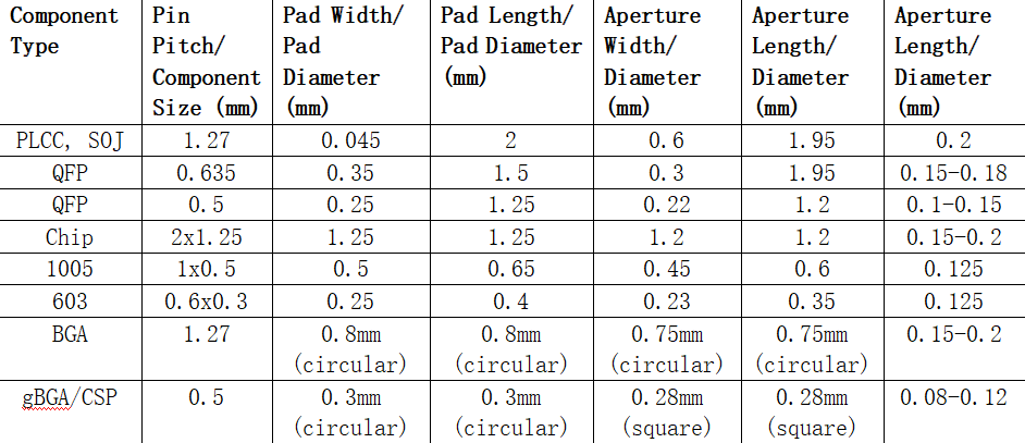
Experience has shown that the amount of solder paste on the pads of general SMT components should be ensured to be around 0.8mg/mm², and around 0.5mg/mm² for narrow-pitch components. Too much can easily lead to problems such as excessive solder consumption and solder bridging, while too little can lead to insufficient solder consumption and inadequate welding strength. The table shown on the cover provides corresponding aperture and stencil template design solutions for different components, which can be used as a reference for design.
We will learn other knowledge about PCB SMT stencil in next new.