
Gold wire position is a component positioning method which is often used in HDI high level PCB. The gold wire is not a pure gold line, but a surface treated line after copper leakage on the circuit board, because the HDI board mostly uses the surface treatment method of chemical gold or immersion gold, so that the surface shows a golden color, that is why it is called "gold wire".
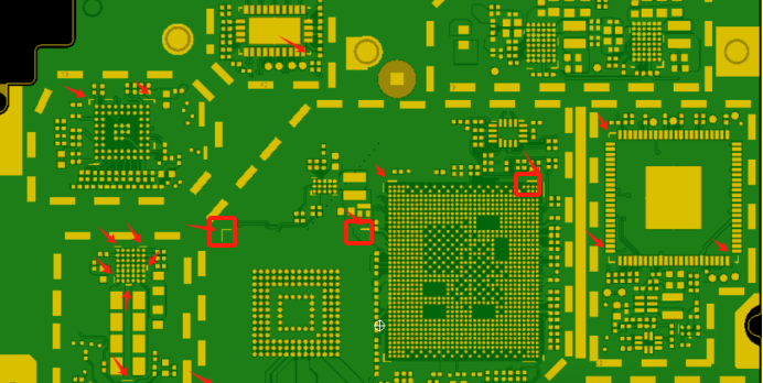
Golden wire position are the red arrows pointed in the picture
Before the gold wire position is applied, the silk screen of the component patch is printed by machine or printed in white oil. As shown in the following picture, the white silk screen is exactly the same as the physical size of the component. After pasting the component, you can judge whether the component is pasted distorted according to the white blockage of the screen frame.
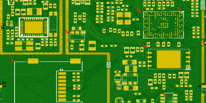
The white blocks in the picture are the silk screen.
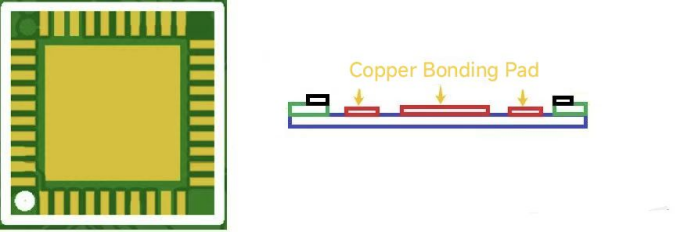
As shown in the following picture, blue indicates the PCB substrate, red indicates the copper foil layer, green indicates the welding resistance green oil layer, black indicates the screen printing layer, the screen printing layer is printed on the green oil layer, so its thickness is greater than the copper foil thickness of the leakage welding pad.

As shown in the following picture, the left side is a Quad Flat No-leads Package (QFN) pad, and the right side is a laminated cross-section diagram. It can be seen that both sides are silk screen lines with high thickness.
What happens if you put in the components? As shown in the following figure, the body of the component first contacts the silk screen on both sides, the component is raised, the pin will not directly contact the pad, and there will be a space between the pad, if the placement is not good, the component may also tilt, so that there will be holes and other poor welding problems during welding.
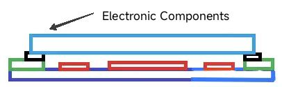
If the pins and spacing of the components are large, these weak problems have little impact on welding, but the components used in the HDI high-density PCB are small in size, and the pin spacing is smaller, and the pin spacing of the Ball Grid Array (BGA) is as small as 0.3mm. After such a small welding problem is superimposed, the probability of poor welding is increased.
Therefore, in the high-density board, many design companies have canceled the screen printing layer, and use the gold thread with copper leakage in the window to replace the screen printing line for positioning, and some Logo ICONS and text also use copper leakage.
This news material is coming from the Internet and is for sharing and communication only.


