
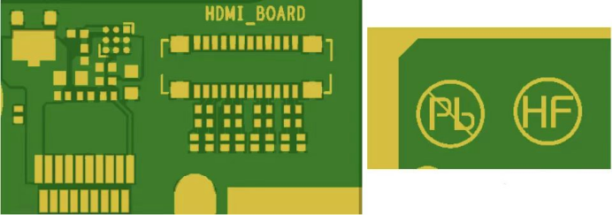
As we all know, the gold wire position process is mainly used in SMT patch factories, so what are the advantages or disadvantages of gold wire position for plate making?
Advantages:
1.Improve the two-dimensional code recognition rate:
In PCB manufacturing, the use of gold wire position can make the width smaller, compared with the minimum width of the silk screen line hollow printing 0.13mm and the screen printer printing minimum width of 0.08mm, the gold wire is not subject to this limitation, the width can be smaller, so that the two-dimensional code recognition rate is higher.
2.Reduce the production cost of the board:
Because there is no screen printing, the board does not need to enter the screen printing process, shortening the process and reducing the production cost.
Disadvantages:
1.It is difficult for EDA engineers to build libraries and route:
When the normal process is building the library, the construction engineer needs to add the gold line positioning information, and needs to place an Etch line on Soldmask, which sets obstacles for EDA engineers to walk the line, and the surface line will automatically avoid the Soldmask area, increasing the design difficulty.
2.There is the risk of short circuit:
If the gold wire position is not made in the component library and the gold wire position is temporarily decided, it may not be handled well and lead to many risks, such as causing the short circuit of the gold wire and the next pin, which may increase the risk of short circuit welding between the pad and GND (ground line);
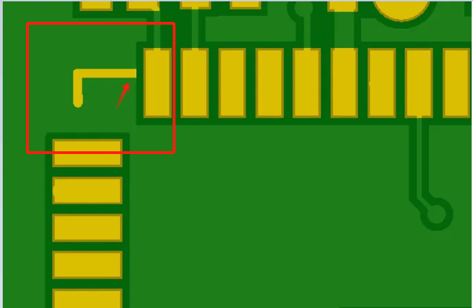
As it shows in the red block
If you do not pay attention to the location of the gold wire, the non-GND wire may leak copper. If the device body is a metal shell, the connection between the wire and GND through the shell will be short-circuit.
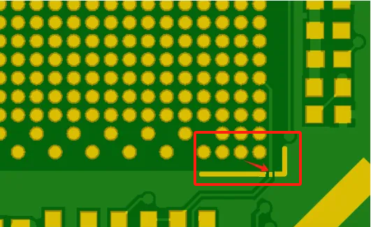
As it shows in the red block
After all, the use of gold wire position needs to be careful, in a hurry, less than review is more likely to cause problems.
This news material is coming from the Internet and is for sharing and communication only.


