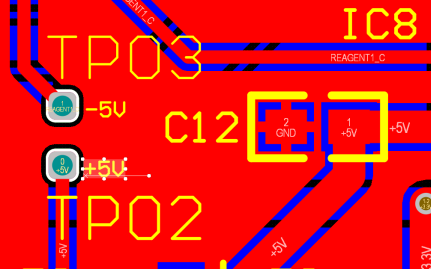

Let's discuss three non-electrical safety clearances: the width, height, and spacing of characters, the spacing between silk screening and pads, and the 3D height and horizontal spacing in mechanical structures.
Character Width, Height, and Spacing:
For silk-screened characters, we typically use standard values such as 5/30 or 6/36 MIL. This is because if the text is too small, it will become blurred and unclear during the printing process.
Silk Screening and Pad Spacing:
Silk screening should not cover pads. If silk screening covers a pad, solder will not adhere to the silk-screened area during the soldering process, which can affect the placement of components. Generally, PCB manufacturers require an 8 MIL clearance. If the PCB panel area is very tight, a 4 MIL clearance is also reluctantly acceptable. If silk screening accidentally covers a pad during design, the manufacturer will automatically remove the silk-screened portion on the pad to ensure solder adhesion. Therefore, it is something we need to pay attention to.
3D Height and Horizontal Spacing in Mechanical Structures:
When components are placed on the PCB, it is important to consider whether there will be any conflicts with other mechanical structures in the horizontal direction or in terms of spatial height. Therefore, in the design phase, it is crucial to fully consider the compatibility of the spatial structure between components, as well as between the finished PCB and the product casing, and to reserve safety clearances for each target object.
All above are the seven types of clearance issues that may be encountered in PCB design. If you would like to learn more specifically, we welcome you to place an order with us.