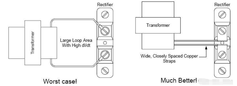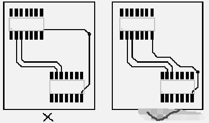

In PCB routing design, ensuring minimal loop area is an important consideration. Loop area refers to the area enclosed by the signal trace and its return path. The size of this loop area directly affects the electromagnetic compatibility (EMC) and radio frequency interference (RFI) of the circuit. A smaller loop area reduces the electromagnetic radiation emitted by the circuit and also the external interference it receives. This is because a small loop area reduces the area of the current loop, thereby reducing the radiation and reception of electromagnetic fields. This is particularly important in high-speed or RF designs, where signal integrity and interference control are crucial for performance.
To achieve this, designers typically strive to shorten the length of signal traces and ensure that the return path is as close as possible to the signal trace to form a tight loop. Additionally, using ground planes and ground grids can provide a good return path, helping to minimize loop area.
