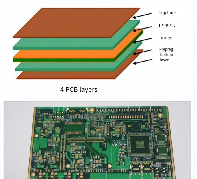

Today, we continue to discuss multilayer PCB, the four-layer PCB
A four-layer PCB is a printed circuit board with four conductive layers: the top layer, two inner layers, and the bottom layer. The two inner layers are cores, typically used as power or ground planes, while the top and bottom outer layers are used for placing components and routing signals.
The outer layers are usually covered with a solder mask layer with exposed pads to provide mounting points for connecting surface-mount devices and through-hole components. Through-holes are typically used to provide connections between the four layers, forming a single board when they are laminated together.
Here is a breakdown of these layers:
First layer: The bottom layer, usually made of copper. It serves as the foundation for the entire circuit board, providing support for the other layers.
Second layer: The power layer. It is named as such because it provides a clean and stable power supply to all components on the circuit board.
Third layer: The ground plane layer, acting as the grounding source for all components on the circuit board.
Fourth layer: The top layer is used for routing signals and providing connection points for components.
The cover image shows the layout of a standard 4-layer PCB stack-up, which can also be modified according to customer requirements.
In the next new, we will learn about the structure, advantages, and application of six-layer PCB.