
In this new, we will learn about the knowledge of single-layer PCB and double-sided PCB.
1. Single-layer PCB
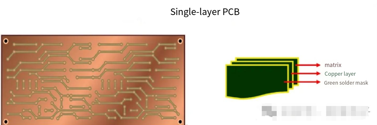
The construction of a single-layer PCB is quite simple. A single-layer PCB consists of a layer of laminated and welded dielectric conductive material layers. It is first covered with a copper layer and then covered with a solder mask layer. An illustration of a single-layer PCB typically shows three color bands to represent the layer and its two covering layers - gray represents the dielectric layer itself, brown represents the copper cladding, and green represents the solder mask layer. (As shown in the cover image)
The advantage of a single-layer PCB is the low cost of manufacture. Especially for the production of consumer devices, the cost-effectiveness is high, and components are relatively simple to drill, weld, and install, making production issues less likely. It is economical and suitable for large-scale production quantities. Ideal for low-density designs.
The main application areas for single-layer PCBs are some everyday small electronic devices. For example, calculators, the most basic calculators use single-layer PCBs. Radios are another example, such as low-priced radio alarms found in general merchandise stores, which typically use single-layer PCBs. Coffee machines also commonly use single-layer PCBs.
2.Double-sided PCB
A double-sided PCB has copper plating on both sides, with an insulating layer in between, and components on both sides of the board, which is why it is also called a double-sided PCB. They are manufactured by connecting two layers of copper together with a dielectric material in between, where each side of the copper can carry different electrical signals, making them suitable for applications requiring high speed and compact packaging.
Electrical signals are routed between the two layers of copper, and the dielectric material between them helps prevent these signals from interfering with each other. The 2-layer PCB is the most common and is the most economical to manufacture.
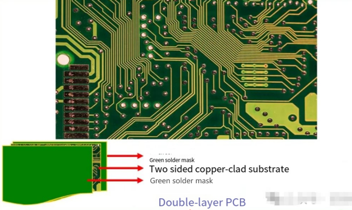
A double-sided PCB is similar to a single-layer PCB but with an inverted mirror image on the bottom half. With a double-sided PCB, the dielectric layer is thicker than a single layer. Additionally, the dielectric is laminated with copper on both the top and bottom. Moreover, both the top and bottom of the laminate are covered with a solder mask layer. An illustration of a double-sided PCB typically looks like a three-layer sandwich, with a thick gray layer in the middle representing the dielectric, top and bottom brown strips representing copper, and thin green strips on the top and bottom representing the solder mask layer, as shown in the picture above.
Advantages: The flexibility of design makes it suitable for a variety of devices. The low-cost structure makes it convenient for mass production. The simple and compact design is suitable for various devices.
Applications: Double-sided PCBs are suitable for a variety of simple and more complex electronic devices. Examples of mass-produced devices containing double-sided PCBs include: HVAC devices, various brands of residential heating and cooling systems contain double-layer printed circuit boards. Amplifiers, double-sided PCBs are equipped with amplifier units used by many musicians. Printers, various computer peripherals rely on double-sided PCBs.
In the next article, we will analyze other multi-layer PCB features.


