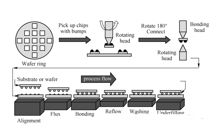

Let’s continue to learn the the process about chip placement.
As shown in the cover picture.
1. Pick-up Chips with Bumps:
In this step, the wafer has been diced into individual chips, adhered to a blue film or UV film. When picking up the chips is required, the pins extend from the bottom, gently pushing against the back of the chip, slightly lifting it. At the same time, the vacuum nozzle accurately picks up the chip from above, thus detaching the chip from the blue film or UV film.
2. Chip Orientation:
After the chip is picked up by the vacuum nozzle, it is passed to the Bonding Head, and during the handoff, the orientation of the chip is changed so that the side with the bumps faces downward, ready to align with the substrate.
3. Chip Alignment:
The rotated chip's bumps are precisely aligned with the pads on the packaging substrate. Alignment accuracy is crucial to ensure that each bump accurately aligns with the pad position on the substrate. Flux is applied to the pads on the substrate, which serves to clean, reduce surface tension on the solder balls, and promote the flow of solder.
4. Chip Bonding:
After alignment, the chip is gently placed on the substrate by the Bonding Head, followed by the application of pressure, temperature, and ultrasonic vibration, which causes the solder balls to settle on the substrate, but this initial bond is not strong.
5. Reflow:
The high temperature of the reflow soldering process melts and flows the solder balls, creating a tighter physical contact between the chip's bumps and the substrate's pads. The temperature profile for reflow soldering consists of preheating, soaking, reflow, and cooling stages. As the temperature drops, the molten solder balls resolidify, significantly strengthening the bond between the solder balls and the substrate pads.
6. Washing:
After reflow soldering is completed, there will be residual flux adhering to the surfaces of the chip and substrate. Therefore, a specific cleaning agent is needed to remove the flux residue.
7. Underfilling:
Epoxy resin or similar material is injected into the gap between the chip and the substrate. The epoxy resin primarily acts as a buffer to prevent cracks in the bumps due to excessive stress during subsequent use.
8. Molding:
After the encapsulant material has cured at the appropriate temperature, the molding process is carried out, followed by reliability testing and other inspections, completing the entire chip encapsulation process.
That is all the information about flip chip in SMT technique. If you want to learn more, just take an order with us.